Manufacturing method of sapphire lens substrate
A production method, sapphire technology, applied in the direction of manufacturing tools, stone processing equipment, fine working devices, etc., can solve the problems of low efficiency and low yield of processing methods, and achieve simple and beautiful appearance, high yield and cost saving Effect
- Summary
- Abstract
- Description
- Claims
- Application Information
AI Technical Summary
Problems solved by technology
Method used
Image
Examples
Embodiment 1
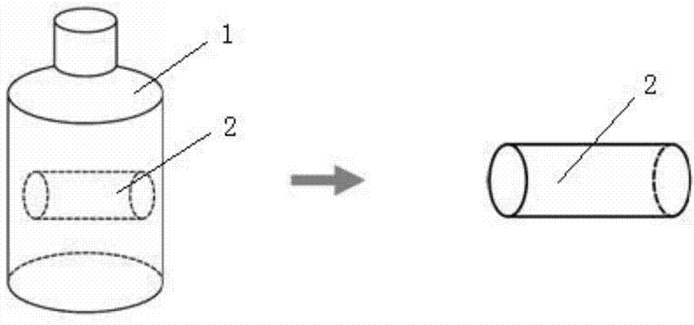
[0044] 1. After the orientation of the crystal ball is completed, the crystal ball is processed into a cylindrical ingot with a diamond barrel cutter, and the crystal direction of the ingot is selected as C direction;
[0045] The inner diameter of the barrel cutter used is 59mm, the outer diameter is 65mm, the diamond grit is 80um, and the spindle speed is 300rpm;
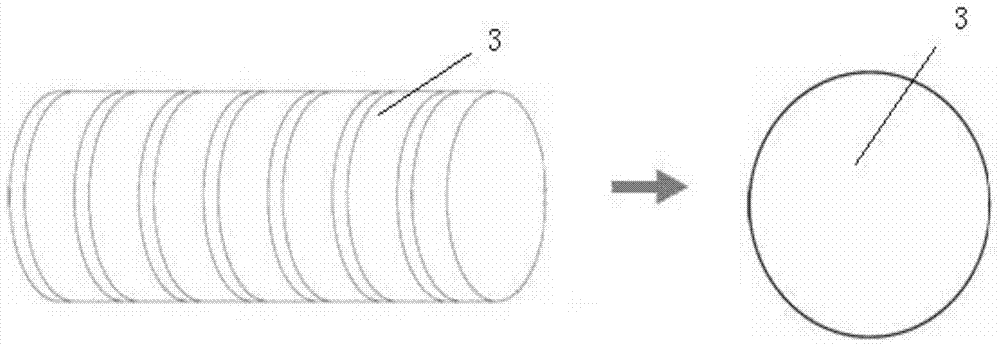
[0046] 2. Use a diamond wire saw to cut the cylindrical ingot into discs with a thickness of 0.3mm and a diameter of 55mm;
[0047] 3. Surface treatment of circular wafers by grinding and polishing to meet the requirement of roughness Ra≤5nm;
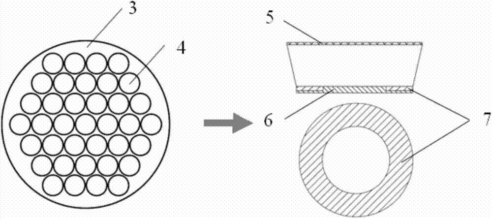
[0048] 4. Use laser cutting to cut the sapphire wafer into a conical camera substrate. The diameter of the camera substrate is 5mm and the thickness is 0.3mm; the laser cutting removal amount of the wafer is 5um, and the cutting speed is 10mm / s.
[0049] The utilization rate of raw materials is 96.1%. It takes 109.96s to cut a wafer, and 70PCS of camera substrates are cut ...
Embodiment 2
[0051] 1. After the orientation of the crystal ball is completed, the crystal ball is processed into a cylindrical ingot with a diamond barrel cutter, and the crystal direction of the ingot is selected as C direction;
[0052] The inner diameter of the barrel cutter used is 51mm, the outer diameter is 58mm, the diamond grit is 70um, and the spindle speed is 280rpm;
[0053] 2. Use a diamond wire saw to cut the cylindrical ingot into discs with a thickness of 0.7mm and a diameter of 48mm;
[0054] 3. Surface treatment of circular wafers by grinding and polishing to meet the requirement of roughness Ra≤5nm;
[0055] 4. Use laser cutting to cut the sapphire wafer into a cylindrical camera substrate. The diameter of the camera substrate is 7mm and the thickness is 0.7mm; the laser cutting removal volume of the wafer is 3um, and the cutting speed is 8mm / s.
[0056] The utilization rate of raw materials is 97.2%. It takes 65.98s to cut a wafer, and 24PCS of camera substrates are cu...
Embodiment 3
[0058] 1. After the orientation of the crystal ball is completed, the crystal ball is processed into a cylindrical ingot with a diamond barrel cutter, and the crystal direction of the ingot is selected as C direction;
[0059] The inner diameter of the barrel cutter used is 55mm, the outer diameter is 62mm, the diamond grit is 75um, and the spindle speed is 290rpm;
[0060] 2. Use a diamond wire saw to cut the cylindrical ingot into discs with a thickness of 0.5mm and a diameter of 52mm;
[0061] 3. Surface treatment of circular wafers by grinding and polishing to meet the requirement of roughness Ra≤5nm;
[0062] 4. Use laser cutting to cut the sapphire wafer into a frustum-shaped camera substrate. The diameter of the camera substrate is 7mm and the thickness is 0.5mm; the laser cutting removal volume of the wafer is 4um, and the cutting speed is 9mm / s.
[0063] The utilization rate of raw materials is 95.7%. It takes 73.3s to cut a wafer, and 30PCS of camera substrates are cu...
PUM
| Property | Measurement | Unit |
|---|---|---|
| thickness | aaaaa | aaaaa |
| diameter | aaaaa | aaaaa |
| diameter | aaaaa | aaaaa |
Abstract
Description
Claims
Application Information


