Array substrate and manufacturing method and display device thereof
A technology for array substrates and display devices, applied in semiconductor/solid-state device manufacturing, electrical components, electric solid-state devices, etc., can solve problems such as structural defects and other structural defects of organic insulating layers
- Summary
- Abstract
- Description
- Claims
- Application Information
AI Technical Summary
Problems solved by technology
Method used
Image

Examples
Embodiment 1
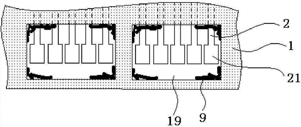
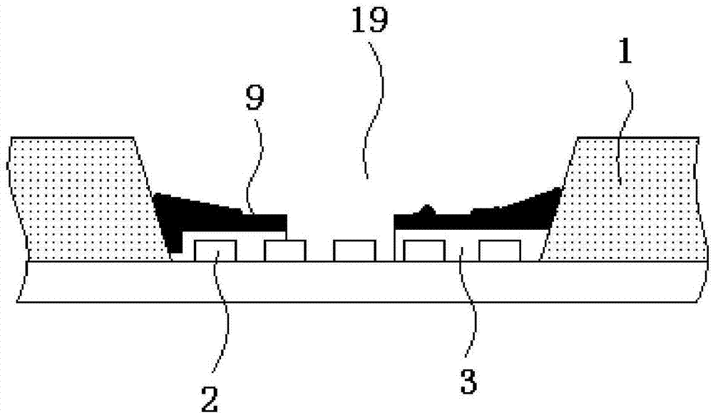
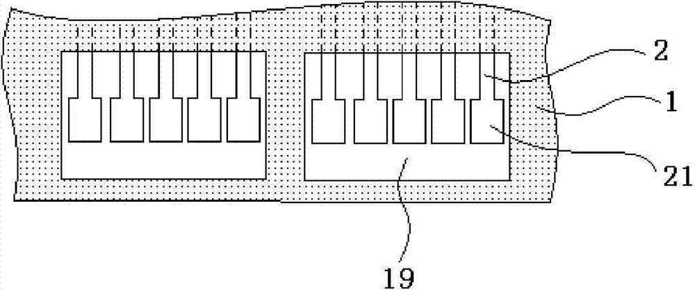
[0030] Such as image 3 , Figure 4 As shown, the present embodiment provides an array substrate, which includes an insulating layer, and the opening 19 is provided in the insulating layer.
[0031] The array substrate of this embodiment may be an array substrate used in liquid crystal display devices, organic light emitting diode display devices, and the like. The array substrate includes many insulating layers for separating structures of different layers, and at least one of these insulating layers is provided with an opening 19 (or called a via hole) for electrically connecting the upper and lower structures.
[0032] Wherein, the insulating layer includes: a first insulating layer; a second insulating layer disposed on the first insulating layer, and the slope angle of the second insulating layer 12 at the opening 19 is smaller than the slope angle of the first insulating layer 11 .
[0033] More preferably, the above insulating layer is the organic insulating layer 1 ,...
Embodiment 2
[0060] This embodiment provides a method for preparing the above-mentioned array substrate, which includes:
[0061] A first insulating layer and a second insulating layer are formed, and openings are formed in the first insulating layer and the second insulating layer.
[0062] Preferably, the above steps of forming the first insulating layer and the second insulating layer, and forming openings in the first insulating layer and the second insulating layer specifically include:
[0063] forming a first insulating layer;
[0064] forming a second insulating layer;
[0065] At the same time, openings are formed through the first insulating layer and the second insulating layer.
[0066] That is to say, after the first insulating layer and the second insulating layer are formed first, openings are formed in the two layers at the same time, thereby simplifying the process. Of course, it is also feasible to form the first insulating layer first and form the opening therein, and...
Embodiment 3
[0071] This embodiment provides a display device, which includes the above-mentioned array substrate.
[0072] Specifically, the display device provided in this embodiment can be any product or component with a display function such as a liquid crystal display panel, an electronic paper, an OLED panel, a mobile phone, a tablet computer, a television set, a monitor, a notebook computer, a digital photo frame, and a navigator.
PUM
 Abstract
Description
Claims
Application Information
 - R&D
- Intellectual Property
- Life Sciences
- Materials
- Tech Scout
- Unparalleled Data Quality
- Higher Quality Content
- 60% Fewer Hallucinations
Browse by: Latest US Patents, China's latest patents, Technical Efficacy Thesaurus, Application Domain, Technology Topic, Popular Technical Reports.
© 2025 PatSnap. All rights reserved.Legal|Privacy policy|Modern Slavery Act Transparency Statement|Sitemap|About US| Contact US: help@patsnap.com