Carrier structure with side pads and manufacturing method thereof

A manufacturing method and carrier board technology, which is applied in the coupling of optical waveguides, light guides, optics, etc., can solve the problems of high cost, high price, and the maturity of flexible printed circuit boards less than rigid printed circuit boards, etc., to achieve cost Low, easy-to-process, and easy-to-assemble effects

Active Publication Date: 2017-03-22
NAT CENT FOR ADVANCED PACKAGING CO LTD
View PDF9 Cites 3 Cited by
  • Summary
  • Abstract
  • Description
  • Claims
  • Application Information

AI Technical Summary

Problems solved by technology

[0004] Another method is to use a flexible printed circuit board or a rigid-flexible hybrid board composed of a flexible printed circuit board and a rigid printed circuit board, and use the flexible printed circuit board's bendable characteristics to bend the flexible printed circuit board. 90 degrees to realize the 90-degree turn of the circuit, such as the US patent "Fiber Optic Connections and Method for Using Same" (patent number: US 6712527 B1), but the production maturity of flexible printed circuit boards is far less than that of rigid printed circuit boards At present, the number of layers of flexible printed circuit boards is not many (2-4 layers), and the high-frequency characteristics of the board are not as good as the rigid board, and the price is more expensive and the cost is higher.

Method used


Image

  • Carrier structure with side pads and manufacturing method thereof
  • Carrier structure with side pads and manufacturing method thereof
  • Carrier structure with side pads and manufacturing method thereof

Examples


Embodiment Construction

[0043] The technical solutions of the present invention will be further described below in conjunction with the accompanying drawings and through specific implementation methods.

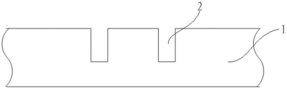
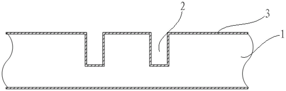
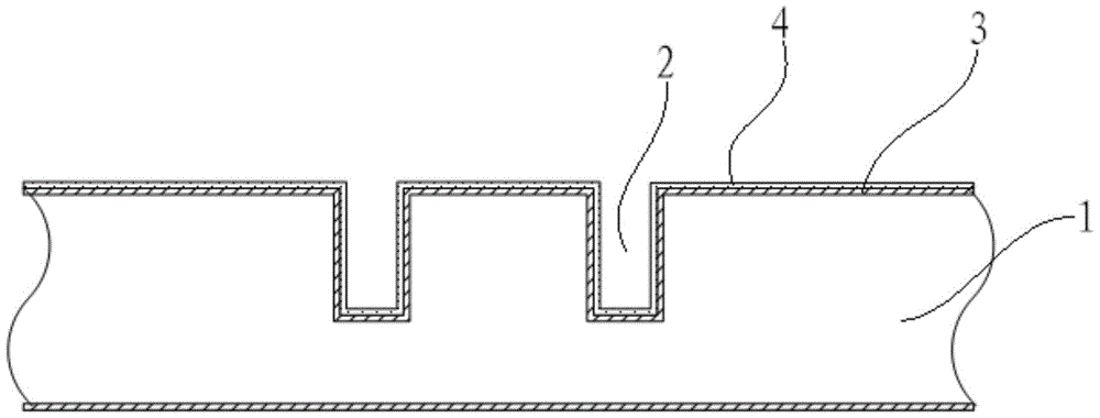
[0044] see Figure 1 to Figure 12 As shown, in this embodiment, a method for manufacturing a carrier board with side pads includes the following steps:

[0045] 1) Etching two rectangular grooves 2 on the silicon wafer 1, the rectangular grooves 2 are arranged in parallel and at intervals;

[0046] 2) Etching one side of the rectangular groove 2 on the silicon wafer 1 and growing a silicon dioxide insulating layer 3 by thermal oxidation;

[0047] 3) growing an electroplating seed layer 4 on the surface of the silicon dioxide insulating layer 3;

[0048] 4) Electroplate copper on the surface of the electroplating seed layer 4, etch one side of the rectangular groove 2 on the silicon wafer 1 and form a copper layer 5 in the rectangular groove 2. The copper layer 5 does not need to be fully plated, b...


PUM


Abstract

The invention discloses a load board structure with a side welding plate and a manufacturing method of the load board structure. The manufacturing method includes the following steps of 1), etching rectangular grooves; 2), growing an insulation layer; 3), growing an electroplating seed layer; 4), performing copper plating; 5), subjecting to a copper layer to imaging; 6), passivating the insulation layer on the surface of the copper layer; 7), etching a carrier between every two neighboring rectangular grooves, a silicon dioxide insulation layer and the electroplating seed layer out of the side face of the copper layer; 9), performing surface processing on exposed copper layer; 10), performing scribing; 11), wire welding gold lines. The manufacturing method of a load board is standard and stable in technology, low in cost, easy to process and suitable for mass production.

Description

technical field [0001] The invention belongs to the technical field of optoelectronic packaging, and in particular relates to a carrier plate structure with side pads and a manufacturing method thereof. Background technique [0002] The vertical cavity surface emitting laser (VCSEL) and the surface photodetector are directly aligned and coupled with the optical fiber. Although the coupling efficiency is high, the direction of the fiber is perpendicular to the vertical cavity surface emitting laser (VCSEL) and the surface photodetector; usually, the vertical cavity surface The upper and lower surfaces of the emitting laser (VCSEL) and the surface receiving detector are parallel to the plane of the circuit board, so the direction of the optical fiber and the surface of the circuit board are perpendicular to each other at this time; due to the limited bending radius, especially the bending half of the optical fiber ribbon is relatively large. The application scenario of this co...

Claims


Application Information

Patent Timeline
Patent Type & Authority Patents(China)
IPC IPC(8): G02B6/42
CPCG02B6/4257G02B6/428
Inventor 薛海韵李宝霞
Owner NAT CENT FOR ADVANCED PACKAGING CO LTD
Why Eureka
Try Eureka