Double-face hardened film and capacitance touch screen with double-face hardened film
A hardened film, double-sided technology, applied in the direction of electrical digital data processing, input/output process of data processing, instruments, etc., can solve the problem of obvious three-dimensional lines on the double-sided hardened film, so as to avoid the obvious color difference and reduce deformation degree, improve the effect of three-dimensional lines
- Summary
- Abstract
- Description
- Claims
- Application Information
AI Technical Summary
Problems solved by technology
Method used
Image
Examples
Embodiment 1
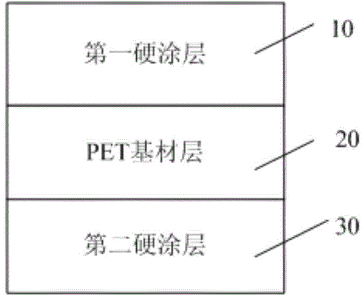
[0043] First, a PET base material layer is provided, and the shrinkage rate of the PET base material layer in the machine direction is 0.5%, and the shrinkage rate perpendicular to the stretching direction is 0.05%.
[0044] Carry out the preparation of the second hard coat layer then, join hardening solution (Arakawa, Japan: FZ001) in the methyl isobutyl ketone solvent and stir for 1 hour, control the solid content (active ingredient content) of hardening solution to be 30%, by coating process, forming a second hard coat layer with a thickness of 2.0 μm on one surface of the PET substrate layer.
[0045] Next, a first hard coat layer was provided on the surface of the PET substrate layer away from the second hard coat layer.
[0046] Mix silicon dioxide particles with a particle size of 50nm and a hardening solution (Arakawa, Japan: FZ001), and add the mixed solution into a methyl isobutyl ketone solvent and stir for 1 hour, and control the solid content of the mixed solution...
Embodiment 2
[0049] The same process as in Example 1 was used to form the double-sided cured film of Example 2. The specific structural parameters of the double-sided cured film are shown in Table 1, and the three-dimensional pattern effect and haze are shown in Table 2.
Embodiment 3
[0051] The double-sided cured film was formed by the same process as in Example 1. The specific structural parameters of the double-sided cured film are shown in Table 1, and the three-dimensional pattern effect and haze are shown in Table 2.
PUM
| Property | Measurement | Unit |
|---|---|---|
| thickness | aaaaa | aaaaa |
| thickness | aaaaa | aaaaa |
| thickness | aaaaa | aaaaa |
Abstract
Description
Claims
Application Information


