Substrate structure and fabrication method thereof

一种基板、制法的技术,应用在具有绝缘保护层的基板结构及其制法领域,能够解决电性接触垫100固定力不佳、防焊层11碎裂、短路等问题,达到避免龟裂与不良的效果

Inactive Publication Date: 2015-07-29
SILICONWARE PRECISION IND CO LTD
View PDF5 Cites 5 Cited by
  • Summary
  • Abstract
  • Description
  • Claims
  • Application Information

AI Technical Summary

Problems solved by technology

[0006] However, when the solder ball 13 is reflowed, the solder ball 13 will thermally expand due to heating, and the solder of the solder ball 13 will extend and diffuse along the path of the circuit 101 and flow into the bottom of the solder resist layer 11, and Since the materials of the solder resist layer 11 and the solder ball 13 are different, the solder resist layer 11 is cracked (Crack) due to the difference in coefficient of thermal expansion (Coefficient of Thermal Expansion, CTE), as shown in the figure K
[0007] In addition, since the solder resist layer 11 is prone to cracks, the chemicals in the process will contact the substrate body 10 through the cracks K, thereby contaminating the substrate body 10.
Or, water vapor will enter the substrate body 10 from the cracked part K, causing problems such as oxidation or short circuit of the circuit 101
[0008] In addition, when conducting reliability tests (such as high-temperature storage, drop tests, etc.), it is easy to produce stress changes from the cracks K of the solder resist layer 11, resulting in large-scale cracks and defects in the solder resist layer 11. question
[0009] In addition, although the method of enlarging the opening 110 can be used to completely expose the electrical contact pad 100 to the opening 110' (that is, the diameter R' of the opening 110' is greater than the width A of the electrical contact pad 100, like figure 1 ') to prevent the solder of the solder ball 13 from flowing into the bottom of the solder resist layer 11 along the path of the circuit 101, but if the aperture R' of the opening 110' is too small, the solder ball 13 will still expand due to heat. Squeezing the solder resist layer 11 causes the solder resist layer 11 to crack, and in the subsequent process, the whole layer of the solder resist layer 11 has large-scale cracks and defects. However, if the hole is opened for this 110' continues to expand, it will cause the wiring space of the substrate body 10 to be reduced and not enough for use, and the fixing force of the electrical contact pad 100 is not good and it is easy to fall off.
[0010] On the other hand, similarly, the solder ball 13 will also have the same problem on the semiconductor chip

Method used


Image

  • Substrate structure and fabrication method thereof
  • Substrate structure and fabrication method thereof
  • Substrate structure and fabrication method thereof

Examples


Embodiment Construction

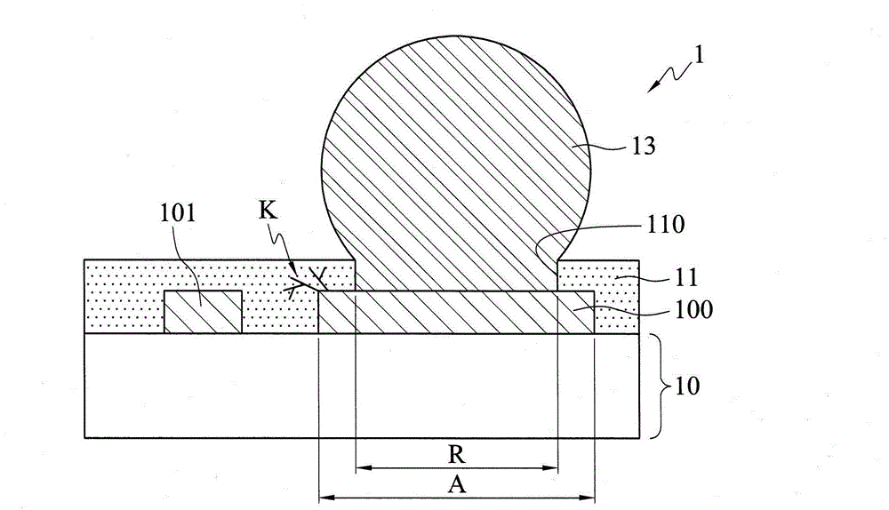
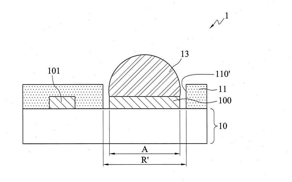
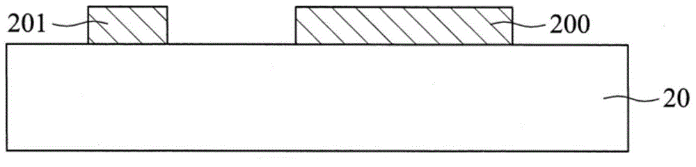
[0046] The implementation of the present invention will be described below through specific examples, and those skilled in the art can easily understand other advantages and effects of the present invention from the content disclosed in this specification.

[0047] It should be noted that the structures, proportions, sizes, etc. shown in the drawings attached to this specification are only used to match the content disclosed in the specification, for the understanding and reading of those skilled in the art, and are not used to limit the implementation of the present invention. Limiting conditions, so there is no technical substantive meaning, any modification of structure, change of proportional relationship or adjustment of size, without affecting the effect and purpose of the present invention, should still fall within the scope of the present invention. The disclosed technical content must be within the scope covered. At the same time, terms such as "above" and "a" quoted ...


PUM


Abstract

A substrate structure is provided, which includes: a substrate body having a plurality of conductive pads; an insulating layer formed on the substrate body and having a plurality of openings for correspondingly exposing the conductive pads; and a plurality of ring bodies formed in the openings and corresponding in position to edges of the conductive pads. As such, a plurality of conductive elements can be subsequently formed inside the ring bodies so as to be prevented by the ring bodies from expanding outward during a reflow process, thereby protecting the insulating layer from being compressed by the conductive elements and preventing cracking of the insulating layer.

Description

technical field [0001] The invention relates to a substrate structure and a manufacturing method thereof, in particular to a substrate structure with an insulating protective layer and a manufacturing method thereof. Background technique [0002] With the evolution of semiconductor packaging technology, different packaging types have been developed for semiconductor devices. Among them, ball grid array (BGA), such as PBGA, EBGA, FCBGA, etc., is an advanced semiconductor packaging technology, which is characterized in that a packaging substrate is used to install semiconductor elements, and the back of the packaging substrate is planted. Place a plurality of solder balls arranged in a grid array, so that more input / output connection terminals (I / O connection) can be accommodated on the same unit area of ​​the carrier to meet the requirements of highly integrated semiconductors The requirements of the chip, and the entire packaging unit is soldered and electrically connected ...

Claims


Application Information

Patent Timeline
Patent Type & Authority Applications(China)
IPC IPC(8): H01L23/488H01L23/498H01L21/48H05K1/02
CPCH05K1/111H01L24/06H01L2224/0401H01L2224/0601H05K1/032H01L2924/384H01L2924/3512H05K2201/0939H01L24/03H05K2201/0154H01L2224/10145H01L23/562H01L23/564H01L24/02H01L24/05H01L24/13H01L24/94H01L2224/02165H01L2224/02235H01L2224/02331H01L2224/05571H01L2224/13021H01L2224/13024H01L2224/131H01L2224/94H01L23/3192H01L23/49816H05K3/3452H05K3/3457H05K2201/09909H05K2203/041H01L2924/351H01L2224/11H01L2924/014
Inventor 张辰安孙崧桓吴建宏陈以婕廖文楷
Owner SILICONWARE PRECISION IND CO LTD
Why Eureka
Try Eureka