Power supply printed circuit board and processing method thereof

A technology for printed circuit boards and processing methods, applied in the directions of printed circuits, printed circuits, printed circuit manufacturing, etc., can solve the problems of large thickness and inconvenience, poor voltage withstand capability of power printed circuit boards, etc., to achieve convenient assembly, Satisfy the effect of high voltage resistance and improve the withstand voltage capability

Inactive Publication Date: 2015-07-29
SHENZHEN SUNTAK MULTILAYER PCB
View PDF6 Cites 18 Cited by
  • Summary
  • Abstract
  • Description
  • Claims
  • Application Information

AI Technical Summary

Problems solved by technology

[0005] The object of the present invention is to provide a processing method of a power printed circuit board, using a soft board copper clad laminate as the inner core board of a power printed circuit board, the soft board copper clad board includes a polyimide base materi

Method used


Image

  • Power supply printed circuit board and processing method thereof
  • Power supply printed circuit board and processing method thereof
  • Power supply printed circuit board and processing method thereof

Examples


Embodiment Construction

[0028] In order to make the object, technical solution and advantages of the present invention clearer, the present invention will be further described in detail below in conjunction with the accompanying drawings and embodiments. It should be understood that the specific embodiments described here are only used to explain the present invention, not to limit the present invention.

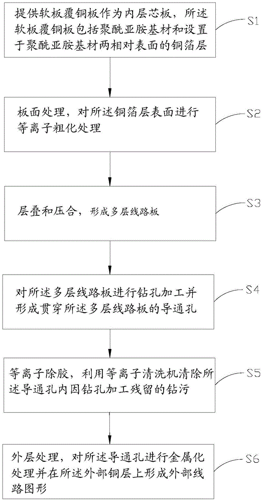
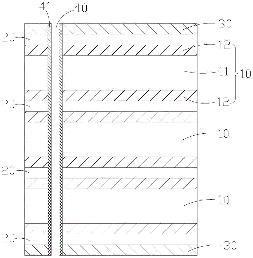
[0029] Please refer to Figure 1 to Figure 3 , the processing method of the power supply printed circuit board provided by the embodiment of the present invention comprises the following steps:

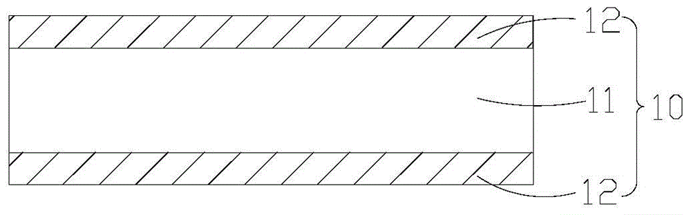
[0030] S1: Provide a flexible copper-clad laminate 10 as an inner core board, the flexible copper-clad laminate 10 includes a polyimide substrate 11 and copper foil layers 12 disposed on two opposite surfaces of the polyimide substrate 11, The copper foil layer 12 is a rolled copper foil, and the copper foil layer 12 is processed by internal pattern transfer to form an internal circuit pattern (not shown)...


PUM


Abstract

The invention is applied to the technical field of a printed circuit board, and provides a processing method of a power supply printed circuit board and a power supply printed circuit board formed by use of the processing method, for the purpose of solving the problems of poor voltage-withstanding capability of a conventional power supply printed circuit board and inconvenient assembling due to large board thickness in the prior art. The processing method of the power supply printed circuit board comprises the following steps: manufacturing an internal layer core plate, providing a soft plate copper-clad plate as the inside core plate, wherein the soft plate copper-clad plate comprises a polyimide substrate and copper coil layers arranged at the two opposite surfaces of the polyimide substrate; performing plasma coarsening processing on the surfaces of the copper foil layers; performing lamination and pressing to form a multilayer circuit board; performing boring processing on the multilayer circuit board and forming a conducting hole; performing plasma glue removing; and performing metallization processing on the conducting hole and forming an external line graph on an external copper layer. According to the processing method, the soft plate copper-clad plate is taken as the internal layer core plate, the voltage withstanding capability of the soft plate copper-clad plate is improved, and the thickness of the power supply printed circuit board is effectively reduced.

Description

technical field [0001] The invention belongs to the technical field of printed circuit boards, and in particular relates to a processing method of a power supply printed circuit board and a power supply printed circuit board formed by the processing method. Background technique [0002] In the printed circuit board industry, power printed circuit boards are one of the main products processed in the printed circuit board industry, and the application range of multilayer power printed circuit boards is becoming wider and wider. [0003] Power printed circuit boards often pass through large currents. In order to ensure functionality, the inner copper thickness of the product must be thicker to reduce the resistance caused by excessive current and prevent problems such as burning boards; at the same time, the use conditions of power printed circuit boards Strict, it is required to withstand high voltage (above 5000V) and prevent high voltage breakdown to prevent safety accidents...

Claims


Application Information

Patent Timeline
IPC IPC(8): H05K1/02H05K3/00H05K3/46
CPCH05K1/032H05K3/022H05K2201/0154
Inventor 何淼刘东朱拓张国城
Owner SHENZHEN SUNTAK MULTILAYER PCB
Why Eureka
Try Eureka