A kind of manufacturing method of LED integrated packaging substrate

A manufacturing method and integrated packaging technology, applied in electrical components, circuits, semiconductor devices, etc., can solve the problem of high processing cost, and achieve the effects of low processing cost, good performance and high connection reliability.

Active Publication Date: 2017-10-13
曹先贵
View PDF4 Cites 0 Cited by
  • Summary
  • Abstract
  • Description
  • Claims
  • Application Information

AI Technical Summary

Problems solved by technology

However, when the resin CCL manufacturing process is used, the via hole processing process is the bottleneck. It is difficult to solve the problem of heat dissipation of the LED chip by using the conventional PTH+electroplating+resin plugging process, and the copper paste (or silver paste) filling process is used. Higher processing costs

Method used


Image

  • A kind of manufacturing method of LED integrated packaging substrate
  • A kind of manufacturing method of LED integrated packaging substrate
  • A kind of manufacturing method of LED integrated packaging substrate

Examples


Embodiment 1

[0043] refer to Figure 1 to Figure 10 , the manufacturing process of the LED integrated packaging substrate of this embodiment includes the following steps:

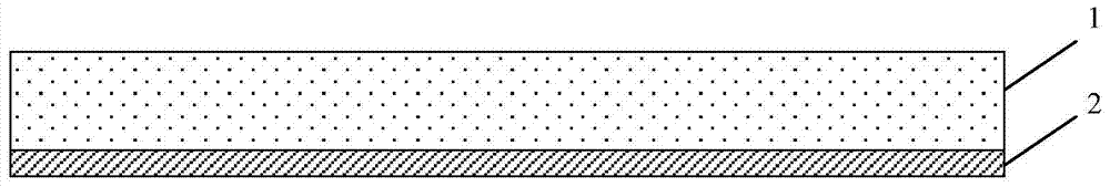
[0044] refer to figure 1 , providing a single-sided copper clad laminate, the copper clad laminate includes a resin layer 1 and a copper layer 2 below the resin layer 1 . The resin layer 1 is made of glass fiber reinforced epoxy resin, and the thickness of the copper layer 2 is above 18um, preferably 25-35um in this embodiment.

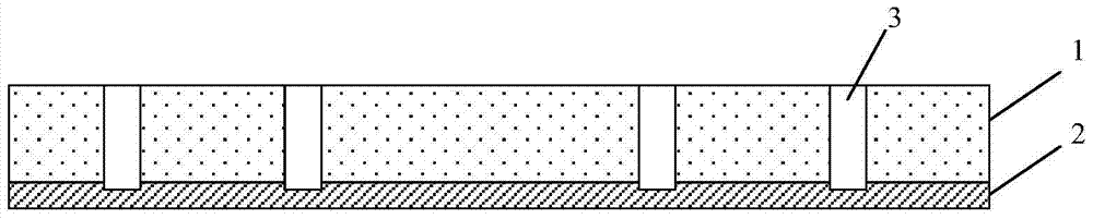
[0045] refer to figure 2 , Drill blind holes on the copper clad board to form via holes 3 . The drilling method can adopt high-precision mechanical positioning drilling or laser drilling blind holes. The via hole 3 penetrates the resin layer 1 from top to bottom in the thickness direction and penetrates into the copper layer 2 without penetrating the copper layer 2 . The position of the via hole 3 is designed according to the customer's design or the position of the LED chip package, wher...

Embodiment 2

[0056] refer to Figure 1-5 and Figure 11-21 , the manufacturing process of the LED integrated packaging substrate of this embodiment includes the following steps:

[0057] Figure 1-Figure 5 The steps shown are the same as in Embodiment 1, and the structures and positional relationships of the formed resin layer 1, copper layer 2, via holes 3, copper pillars 5 and copper terminals 51 are also the same as those in Embodiment 1, and will not be repeated here.

[0058] refer to Figure 11 ,At Figure 5 A polymer conductive film layer 9 is formed on the upper surface of the structure shown, wherein the conductive film layer 9 is formed by depositing colloidal graphite.

[0059] refer to Figure 12 , micro-etching the conductive film layer 9 to remove the conductive film material attached to the surface of the copper terminal 51, so that the subsequent copper electroplating is directly bonded to the copper pillar 5, avoiding the presence of a polymer conductive film between t...

Embodiment 3

[0071] refer to Figure 1-5 and Figure 22-31 , the manufacturing process of the LED integrated packaging substrate of this embodiment includes the following steps:

[0072] Figure 1-Figure 5 The steps shown are the same as in Embodiment 1, and the structures and positional relationships of the formed resin layer 1, copper layer 2, via holes 3, copper pillars 5 and copper terminals 51 are also the same as those in Embodiment 1, and will not be repeated here.

[0073] refer to Figure 22 ,At Figure 5 A titanium-copper conductive film layer 12 is formed on the upper surface of the structure shown, wherein the conductive film layer 12 is formed by physically sputtering two layers of metal titanium and copper, specifically spraying a layer of 40-100nm thick metal titanium layer, and then spraying a layer of metal titanium layer 40-100nm thick on it. Spray a layer of 0.8-3um metal copper layer.

[0074] refer to Figure 23 , form a photosensitive anti-plating etching film 10...


PUM


Abstract

The invention discloses a manufacturing method of an LED integrated package substrate. The manufacturing method comprises the following steps: forming via holes in a resin base single-sided copper-cladding plate through blind hole process, performing electroplating on a copper layer at the bottoms of the via holes to form solid copper columns, forming copper terminals through outward extension of the top ends of the copper columns, and performing exposure, development, etching and other steps through a photosensitive anti-plating etching film to form an LED package substrate finished product. Furthermore, the invention further discloses a double-sided copper-cladding LED package substrate finished product formed with a conductive film to adapt to different requirements of LED power and running temperature environment. According to the method, cost is low, and the manufactured LED integrated package substrate has high heat dissipation performance and high stability and is suitable for practical application.

Description

technical field [0001] The invention relates to a manufacturing process of an LED packaging substrate, in particular to a manufacturing method of an LED integrated packaging substrate. Background technique [0002] For LED packaging applications, in addition to the basic functions of carrying and arranging circuits, the packaging substrate also needs to have the performance of high heat dissipation efficiency. The currently popular LED packaging substrates are mainly made of flexible boards or ceramic substrates, aluminum (metal) substrates, and resin copper clad laminates are rarely used as materials. Compared with metal-based and ceramic-based copper-clad laminates, resin-based copper-clad laminates have low material cost, relatively simple manufacturing process, and strong bonding force with metal copper, so they have good application prospects. However, when the resin CCL manufacturing process is used, the via hole processing process is the bottleneck. It is difficult t...

Claims


Application Information

Patent Timeline
Patent Type & Authority Patents(China)
IPC IPC(8): H01L33/62H01L33/64H01L33/52H01L33/56
CPCH01L33/005H01L33/52H01L33/56H01L33/62H01L33/64
Inventor 曹先贵
Owner 曹先贵
Why Eureka
Try Eureka