Super-junction LDMOS (laterally double-diffused metal-oxide semiconductor) field effect transistor with double-electric-field modulation

A technology of oxide semiconductors and field effect transistors, which is applied to semiconductor devices, circuits, electrical components, etc., can solve problems such as unsatisfactory breakdown voltage of devices, lower BV, and incomplete compensation of SuperJunction charges, so as to optimize electric field distribution and improve Effects of breakdown voltage and low on-resistance

Active Publication Date: 2015-08-12
XIDIAN UNIV
View PDF4 Cites 11 Cited by
  • Summary
  • Abstract
  • Description
  • Claims
  • Application Information

AI Technical Summary

Problems solved by technology

However, many problems have been encountered in the process of realizing SJ-LDMOS, including the substrate-assisted depletion effect SAD (Substrate Assisted Depletion). Adjacent P-pillars and P-type substrates are assisted in depletion, resulting in incomplete com

Method used


Image

  • Super-junction LDMOS (laterally double-diffused metal-oxide semiconductor) field effect transistor with double-electric-field modulation
  • Super-junction LDMOS (laterally double-diffused metal-oxide semiconductor) field effect transistor with double-electric-field modulation

Examples


Embodiment Construction

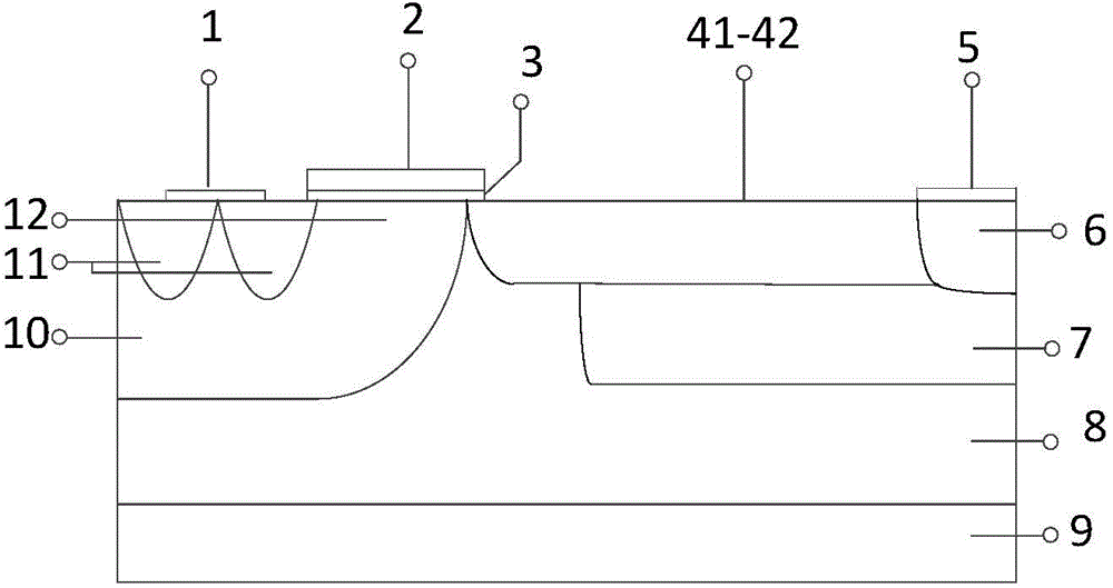
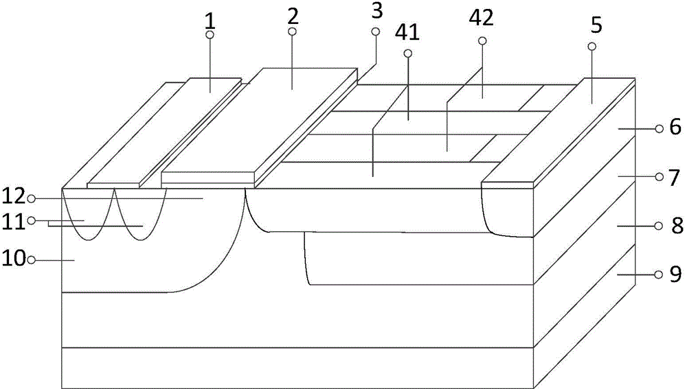
[0028] Such as figure 1 As shown, the structure of the present invention is a lateral superjunction double-diffused metal-oxide-semiconductor field-effect transistor with dual electric field modulation comprising:

[0029] a substrate 9 of semiconductor material;

[0030] an epitaxial layer 8 on the substrate;

[0031] The left end of the epitaxial layer is the base region 10, the middle part is part of the buffer layer 7, and the right end is the drain region 6;

[0032] The upper left end of the base region 10 is the source region 11, and the source region is the source electrode 1;

[0033] On the right end of the base region 10 is a channel 12 , on the channel is a gate insulating layer 3 , on the gate insulating layer 3 is a gate electrode 2 , and on the drain region 6 is a drain electrode 5 .

[0034] Applying Super Junction to LDMOS can effectively reduce the on-resistance of the drift region. And because there is a buffer layer under the Super Junction, the substra...


PUM


Abstract

The invention proposes an SJ-LDMOS (super-junction LDMOS (laterally double-diffused metal-oxide semiconductor) field effect transistor with double-electric-field modulation) with double-electric-field modulation. In the SJ-LDMOS, a partitioning part in a form of an epitaxial layer projection structure is formed between a buffering layer of SJ drift region and a trench, thereby enabling the edge of the buffering layer to modulate an SJ drift region electric field close to the trench. The length of a P column in the SJ drift region is less than the length of an N column, i.e., the P column being separated from a drain region, thereby preventing the connection of the P column with the drain region from generating a peak electric field, and enabling the edge of the buffering layer to modulate the SJ drift region electric field close to the drain region. Therefore, a part of buffering layer below the SJ drift region and the P column structure at the upper part of the SJ drift region are employed for the modulation of two electric fields at two parts of the drift region of a device, thereby enabling the surface electric field of the device to tend to be uniform, and greatly enlarging a breakdown voltage of the device under the condition of guaranteeing low on resistance of the device.

Description

technical field [0001] The invention relates to the field of semiconductor devices, in particular to a lateral superjunction double-diffused metal oxide semiconductor field effect transistor. Background technique [0002] Lateral double-diffused MOS (Lateral Double-diffused MOS, LDMOS) as a representative of high withstand voltage, low on-resistance lateral power devices are widely used in high voltage integrated circuits (high voltage integrated circuit, HVIC) and smart power integrated circuits (smart power integrated circuit, SPIC). Super Junction SJ (Super Junction) technology can enable a very low on-resistance R under a certain breakdown voltage BV (Breakdown Voltage) ON , is applied to LDMOS to form SJ-LDMOS structure and breaks the limit relationship of traditional power MOS devices. However, many problems have been encountered in the process of realizing SJ-LDMOS, including the substrate-assisted depletion effect SAD (Substrate Assisted Depletion). The auxiliary ...

Claims


Application Information

Patent Timeline
IPC IPC(8): H01L29/06H01L29/78
CPCH01L29/0611H01L29/7816
Inventor 段宝兴曹震袁小宁袁嵩杨银堂
Owner XIDIAN UNIV
Why Eureka
Try Eureka