The structure of igbt chip
A chip and PN junction technology, applied in semiconductor devices, electrical components, circuits, etc., can solve the problems of rising cost and increasing difficulty of subsequent packaging, and achieve the effects of improving reliability, good switching speed, and high reliability
- Summary
- Abstract
- Description
- Claims
- Application Information
AI Technical Summary
Problems solved by technology
Method used
Image

Examples
Embodiment 1
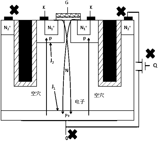
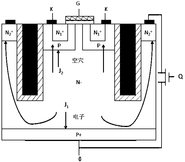
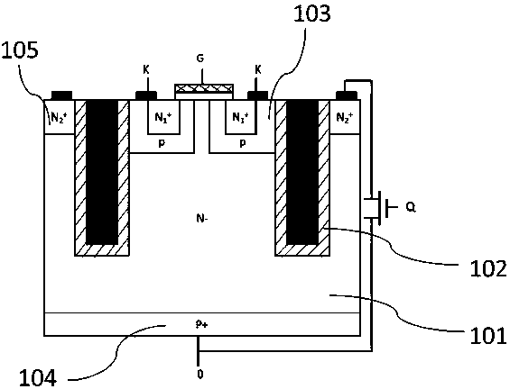
[0028] A structure of an IGBT chip, including an IGBT unit composed of a MOS field effect transistor and a triode, and also includes a control switch Q, an electrode N 2 + and an isolation cover, the IGBT unit is set inside the isolation cover, and the isolation cover is set on the electrode N 2 + Inside, the control switch Q is connected to the electrode N respectively. 2 + It is connected with the triode, when the IGBT unit conducts forwardly, the control switch Q is in the off state, and when the IGBT unit conducts in the reverse direction, the control switch Q is in the open state.
[0029] In this embodiment, when the IGBT unit is in the forward conducting state, the control switch Q is in the closed state, and the PN junction J 2 In reverse bias, J 1 in a forward biased state. That is, as shown in the figure, when the IGBT unit is in forward conduction, the control switch Q is in the closed state, and the PN junction J formed by the P-type channel 103 and the drift...
Embodiment 2
[0039] The present invention is a gate-type high-speed IGBT structure, which introduces an isolation cover, N 2 + and device Q. When the IGBT is in the forward conduction, the PN junction J 2 In the reverse biased state, the PN junction J 1 In the forward-biased state, because of the isolation cover, it plays an isolation role, because there is enough thick insulating material in the isolation cover, for N 2 + There is no effect, so that the IGBT is the same as the traditional IGBT in the forward conduction state, and the direction of the current is as figure 2 So style. When the IGBT is in the reverse direction, J 1 In reverse bias state, J 2 In positive bias, electrons will flow out because of P + The influence of the potential barrier is hindered, and electrons have to overcome the potential barrier block Hard work will generate heat, the more the number of electrons, the greater the heat, which will affect the reliability of the device. Therefore, at present, th...
PUM
 Abstract
Description
Claims
Application Information
 - R&D
- Intellectual Property
- Life Sciences
- Materials
- Tech Scout
- Unparalleled Data Quality
- Higher Quality Content
- 60% Fewer Hallucinations
Browse by: Latest US Patents, China's latest patents, Technical Efficacy Thesaurus, Application Domain, Technology Topic, Popular Technical Reports.
© 2025 PatSnap. All rights reserved.Legal|Privacy policy|Modern Slavery Act Transparency Statement|Sitemap|About US| Contact US: help@patsnap.com