High-voltage spike pulse generating circuit

A technology for generating circuits and narrow pulses, applied in pulse train generators, etc., can solve problems such as inability to effectively turn on NMOS transistors

Active Publication Date: 2015-08-12
NO 24 RES INST OF CETC
View PDF5 Cites 5 Cited by
  • Summary
  • Abstract
  • Description
  • Claims
  • Application Information

AI Technical Summary

Problems solved by technology

[0007] In view of the above-mentioned shortcomings of the prior art, the purpose of the present invention is to provide a high-voltage narrow pulse generating circuit, which is used to solve the problem that the traditional narrow pulse generating circuit in the prior art cannot effectively turn on the NMOS under the extremely low power supply voltage of the deep submicron chip. transistor problem

Method used


Image

  • High-voltage spike pulse generating circuit
  • High-voltage spike pulse generating circuit
  • High-voltage spike pulse generating circuit

Examples


no. 1 example

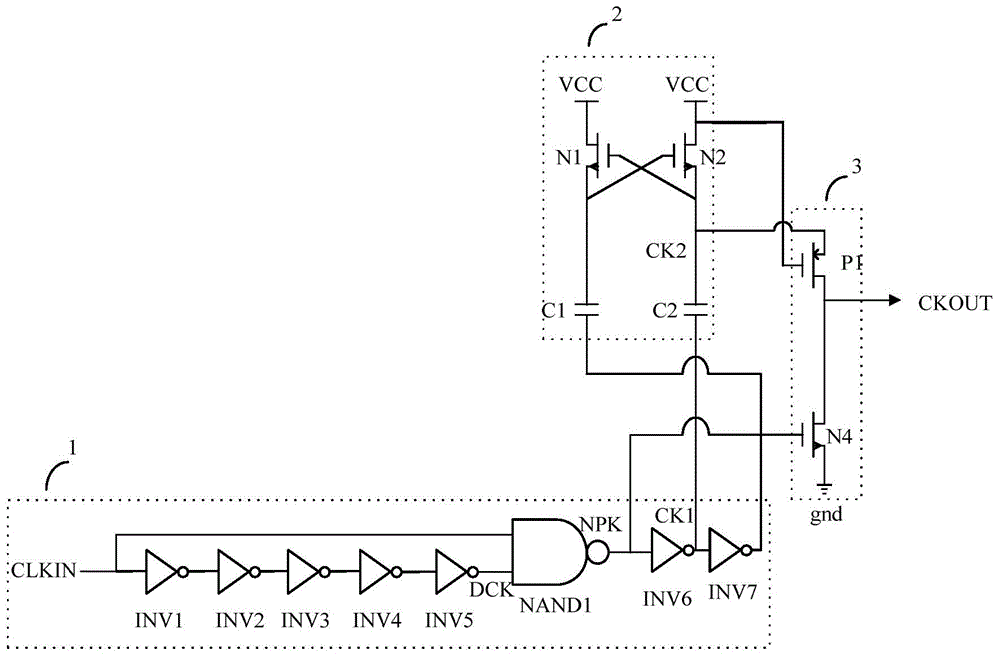
[0043] Circuit of the first embodiment

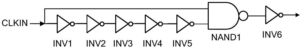
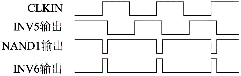
[0044] see image 3 ,Such as image 3 Shown is the circuit of the first embodiment of the high-voltage narrow pulse generating circuit of the invention, the high-voltage narrow pulse generating circuit at least includes a narrow pulse signal generating module 1, a double voltage narrow pulse signal generating module 2 and a high-voltage narrow pulse signal conversion module 3; the narrow pulse The signal generating module is used to generate the first negative narrow pulse signal, the second negative narrow pulse signal and the positive narrow pulse signal, the high level of the positive narrow pulse signal is equal to VCC, the low level is equal to Vgnd, the first negative narrow pulse signal and the second The high level of the negative narrow pulse signal is equal to VCC, and the low level is equal to Vgnd, where VCC is the power supply voltage and Vgnd is the ground voltage;

[0045] The double voltage narrow pulse signal generati...

no. 2 example

[0055] Second embodiment circuit

[0056] Such as Figure 5 It is the circuit of the second embodiment of the present invention. On the basis of the circuit of the first embodiment, the circuit of this embodiment uses other adjustable delay transmission lines to replace the inverters INV1, INV2, INV3, and INV4. After such improvement, the pulse width of the high voltage narrow pulse signal generated by the circuit of the second embodiment is adjustable.

[0057] The narrow pulse signal generating module of this embodiment includes an adjustable delay transmission circuit, a fifth inverter, a sixth inverter, a seventh inverter and a NAND gate;

[0058] The output of the adjustable delay transfer circuit is connected to the input of the fifth inverter; the external clock signal CLKIN is connected to the input end of the adjustable delay transfer circuit and an input end of the NAND gate at the same time; the output end of the fifth inverter is connected to The other input ter...

no. 3 example

[0060] The circuit of the third embodiment

[0061] Such as Image 6 It is the circuit of the third embodiment of the present invention. The circuit of this embodiment is based on the circuit of the first embodiment, and another NMOS transistor, that is, the third transistor N3 is connected in series above the fourth transistor N4. In the circuit of the first embodiment, when the high-voltage narrow pulse CKOUT outputs a high-voltage signal twice the power supply voltage, the drain-source voltage and the drain-gate voltage of the fourth transistor N4 reach 2VCC, such a high inter-electrode voltage It will exceed the breakdown failure of the fourth transistor N4. Image 6Connecting the third transistor N3 in series above the fourth transistor N4 solves this problem. The gate of the third transistor N3 is connected to VCC, the source is connected to the drain of the fourth transistor N4, and the drain is connected to the drain of P1 to output a high voltage narrow pulse signa...


PUM


Abstract

The invention discloses a high-voltage spike pulse generating circuit, at least comprising a spike pulse signal generating module for generating a first negative spike pulse signal, a second negative spike pulse signal and a positive spike pulse signal, a multiplication spike pulse signal generating module for receiving the positive spike pulse signal and the second spike pulse signal, and generating a voltage-multiplying spike pulse signal; and a high-voltage spike pulse conversion module, which is connected with the spike pulse signal generating module and the multiplication spike pulse signal generating module, and is used for receiving the first spike pulse signal and the multiplication spike pulse signal and outputting a high-voltage spike pulse signal. The high-voltage spike pulse generating circuit provided by the invention can be used for generating the high-voltage spike pulse which is twice as the supply voltage in a chip and fully opening an NMOS transistor instantly under the condition of deep submicron supply voltage so as to effectively reset a sampling capacitor in a switched-capacitor circuit. The circuit of the invention solves the problem that a traditional spike pulse generating circuit cannot effectively open the NMOS transistor.

Description

technical field [0001] The invention relates to the field of analog / mixed signal integrated circuits, in particular to a high voltage narrow pulse generating circuit. Background technique [0002] As the feature size of the semiconductor CMOS process develops toward the deep submicron direction, the power supply voltage becomes lower and lower (lower than 1V). Such a low power supply voltage has been unable to effectively turn on / off the MOS transistor. For this reason, it was proposed to generate a voltage signal higher than the power supply voltage inside the chip to solve this problem. Various circuits are designed to generate high-voltage signals higher than the power supply voltage inside the chip, each of which has its own advantages and disadvantages, and each has its own application. [0003] Narrow pulses are widely used in analog / mixed-signal integrated circuits, especially in switched capacitor circuits, to instantly turn on the NMOS transistor and reset the sam...

Claims


Application Information

Patent Timeline
Patent Type & Authority Applications(China)
IPC IPC(8): H03K3/64
CPCH03K3/64
Inventor 胡蓉彬王永禄胡刚毅王育新付东兵张正平李梁
Owner NO 24 RES INST OF CETC
Why Eureka
Try Eureka