CMOS image sensor and method for manufacturing the same

An image sensor and gate technology, applied in semiconductor/solid-state device manufacturing, electrical solid-state devices, semiconductor devices, etc., can solve the problems of miniaturization of difficult products, high power consumption, complex manufacturing process, etc., to improve performance, increase The effect of width

Inactive Publication Date: 2008-07-02
DONGBU HITEK CO LTD
View PDF0 Cites 0 Cited by
  • Summary
  • Abstract
  • Description
  • Claims
  • Application Information

AI Technical Summary

Problems solved by technology

[0004] However, due to the use of multi-level photolithography process, this kind of CCD has the disadvantages of relatively complicated driving method, relatively large power consumption and relatively complicated manufacturing process
[0005] For CCDs, it is also difficult to integrate control circuits, signal processing circuits, and A / D converters on one CCD chip, so CCDs have the disadvantage of making it difficult to miniaturize products.

Method used


Image

  • CMOS image sensor and method for manufacturing the same
  • CMOS image sensor and method for manufacturing the same
  • CMOS image sensor and method for manufacturing the same

Examples


Embodiment Construction

[0019] A CMOS image sensor and a manufacturing method thereof according to an embodiment of the present invention will be described below with reference to the accompanying drawings.

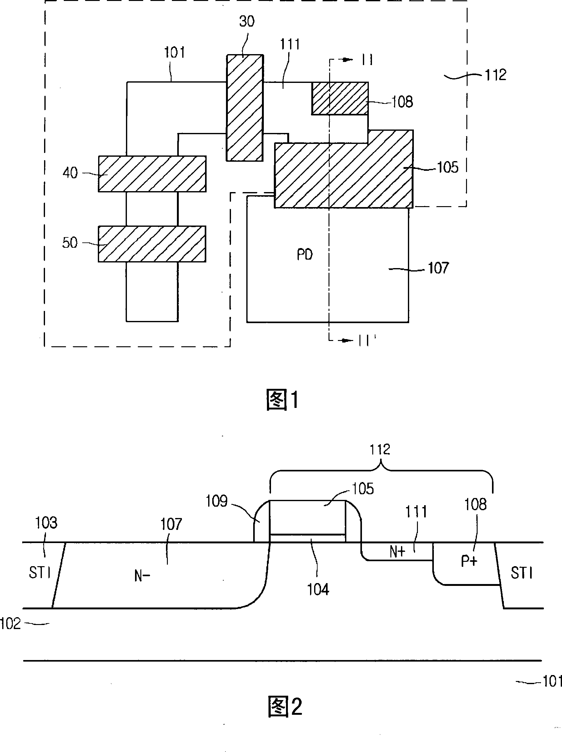
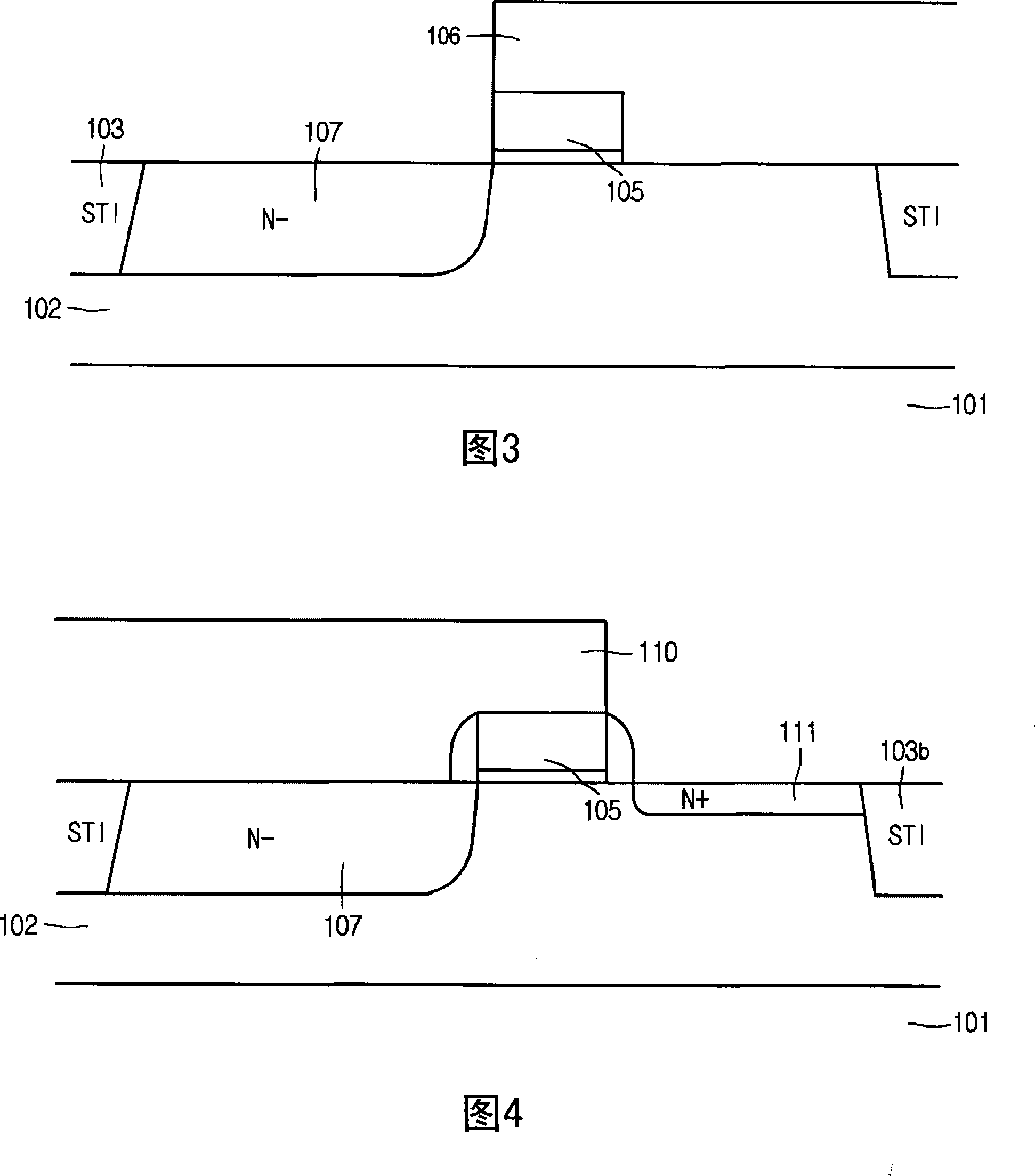
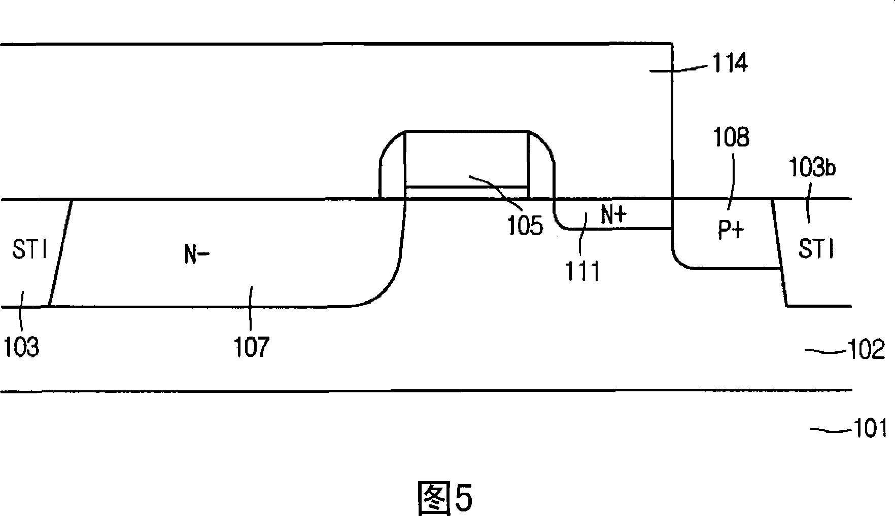
[0020] 1 is a layout diagram illustrating a unit pixel of a CMOS image sensor having a structure including four transistors and one photodiode (PD) according to an embodiment; FIG. 2 is a diagram illustrating the CMOS image sensor in FIG. 1 Sectional view along line II-II'.

[0021] 1 and 2 illustrate one unit pixel including one photodiode PD and four MOS transistors formed on an epitaxial (epi) layer 102 on the surface of a semiconductor substrate 101 (eg, a single crystal silicon wafer). The substrate includes: an active region and a device isolation region (such as STI); a device isolation (isolating) layer 103 is formed in the device isolation region of the semiconductor substrate 101 having an epitaxial layer 102; a gate 105 is formed on the semiconductor On the gate insulating layer 104 ...


PUM


Abstract

The invention discloses a CMOS image sensor and method for manufacturing the same. A CMOS image sensor may include a gate electrode on a gate insulating layer in an active region of a semiconductor substrate; a photodiode region in the semiconductor substrate on one side of the gate electrode; a floating diffusion region in the semiconductor substrate on another side of the gate electrode; and a complementary impurity region in the semiconductor substrate on the other side of the gate electrode, overlapping with the floating diffusion region. Embodiments of the invention relate to a CMOS image sensor and a method for manufacturing the same, adapted to make a reset of a photodiode easy as well as to allow the electrons generated from the photodiode to be easily transferred into a floating diffusion region by making the width of a transfer transistor large and / or the area of a floating diffusion region small, thereby improving the characteristics of the image sensor.

Description

technical field [0001] The present invention relates to a CMOS image sensor and a manufacturing method thereof. Background technique [0002] As a semiconductor device that converts an optical image into an electrical signal, most image sensors are generally classified into charge-coupled devices (CCD) and complementary metal oxide (CMOS) image sensors. [0003] A charge-coupled device (CCD) includes: a plurality of vertical charge-coupled devices (VCCDs) formed between respective vertical photodiodes arranged in an array to vertically transfer charges generated by respective photodiodes; a plurality of photodiodes, arranged in an array, to convert light signals into electrical signals; horizontal charge-coupled devices (HCCDs), to horizontally transfer charges transferred by way of respective vertical charge-coupled devices; and sense amplifiers, to sense the horizontally transferred charge and output it as an electrical signal. [0004] However, due to the use of a multi...

Claims


Application Information

Patent Timeline
Patent Type & Authority Applications(China)
IPC IPC(8): H01L27/146H01L21/822
CPCH01L27/14603H01L27/14689H01L27/14609
Inventor 金升炫
Owner DONGBU HITEK CO LTD
Why Eureka
Try Eureka