
Wafer lifting method

A technology of wafer and lifting movement, applied in the direction of electrical components, semiconductor/solid-state device manufacturing, circuits, etc., can solve problems such as uneven charge distribution, affecting production efficiency and product yield, deviation or chip drop, etc., to reduce deviation or The probability of chip drop, the effect of improving production efficiency and product yield

Inactive Publication Date: 2015-08-26
BEIJING NAURA MICROELECTRONICS EQUIP CO LTD
View PDF5 Cites 4 Cited by
  • Summary
  • Abstract
  • Description
  • Claims
  • Application Information

AI Technical Summary

Problems solved by technology

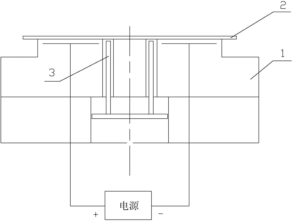
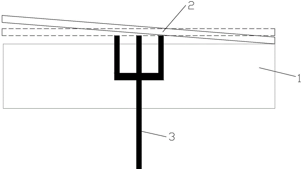
[0005] However, the above method of reducing electrostatic attraction inevitably has the following problems in practical applications, that is, because the above method of reducing electrostatic attraction can only remove charges exposed to the plasma environment, that is, plasma can only remove residual The charge on the upper surface of the wafer 2 cannot remove the charge remaining on the lower surface of the wafer 2 and the upper surface of the base 1, and because the distribution of the residual charge is uneven, when the ejector pin 3 lifts the wafer 2 , wafer 2 will deviate or fall due to uneven force, such as figure 2 As shown, resulting in the interruption of the process, affecting production efficiency and product yield

Method used


Image

  • Wafer lifting method
  • Wafer lifting method
  • Wafer lifting method

Examples


Embodiment Construction

[0027] In order to make those skilled in the art better understand the technical solutions of the present invention, the wafer lifting method provided by the present invention will be described in detail below with reference to the accompanying drawings.

[0028] The wafer lifting method provided by the embodiment of the present invention adopts the existing electrostatic chuck and thimble to realize the lifting of the wafer. The structures of the electrostatic chuck and the thimble have been described in detail in the above background art, and will not be repeated here.

[0029] The wafer lifting method provided by the embodiment of the present invention is used to lift the wafer with an ejector pin after the process is completed, so as to release the wafer from the electrostatic chuck. Among them, after the process is over, it means after the wafer placed on the electrostatic chuck is processed; and, when the wafer is processed, a forward voltage is applied to the electrodes...


PUM


Abstract

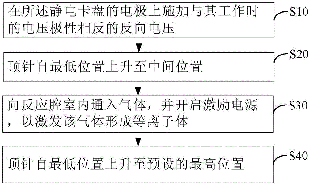
A wafer lifting method provided by the invention is used for jacking up a wafer by means of an ejecting pin after a process so as to enable the wafer to break away from a static chuck. The method comprises the steps that: 10) a reverse voltage opposite to the voltage polarity in work is applied to an electrode of the static chuck so as to reduce the electrostatic attraction between the wafer and the static chuck; 20) the ejecting pin moves up from a lowest position to a middle position to jack up the wafer, so that a preset interval exists between a lower surface of the wafer and an upper surface of the static chuck; 30) gas is pumped into a reaction chamber, an excitation power supply is started to motivate the gas to form plasma, and residual charges on the lower surface of the wafer and the upper surface of the static chuck are eliminated; and 40) the ejecting pin moves from the lowest position to a preset highest position. By adopting the wafer lifting method provided by the invention, the offset or dropping probability of wafer lifting is reduced, so that the production efficiency and the product yield rate are improved.

Description

technical field [0001] The invention relates to the technical field of microelectronics processing, in particular to a wafer lifting method. Background technique [0002] With the rapid development of integrated circuits, the competition among manufacturing enterprises is becoming more and more fierce. Therefore, all manufacturing enterprises are making every effort to reduce production costs and improve production efficiency to improve their competitive advantages. [0003] As we all know, the manufacturing process of integrated circuits is a complex and highly automated assembly process. During processing, the wafer needs to be placed on the chuck for operation, and if the wafer is dislocated or moved during the process of unloading and unloading, or even fragmentation, the entire production process will be interrupted, thereby affecting the production efficiency and product. Yield. Therefore, wafer misalignment, movement or chipping needs to be avoided as much as possib...

Claims


Application Information

Patent Timeline
Patent Type & Authority Applications(China)
IPC IPC(8): H01L21/683
Inventor 管长乐
Owner BEIJING NAURA MICROELECTRONICS EQUIP CO LTD
Learn More