A kind of hollow metal microneedle and batch preparation method thereof
A microneedle and metal technology, applied in the field of medical equipment and biomedicine, can solve the problems of inability to produce micro-sized needles, etc., and achieve the effect of low cost, guaranteed stability, and reasonable microneedle structure
- Summary
- Abstract
- Description
- Claims
- Application Information
AI Technical Summary
Problems solved by technology
Method used
Image
Examples
Embodiment 1
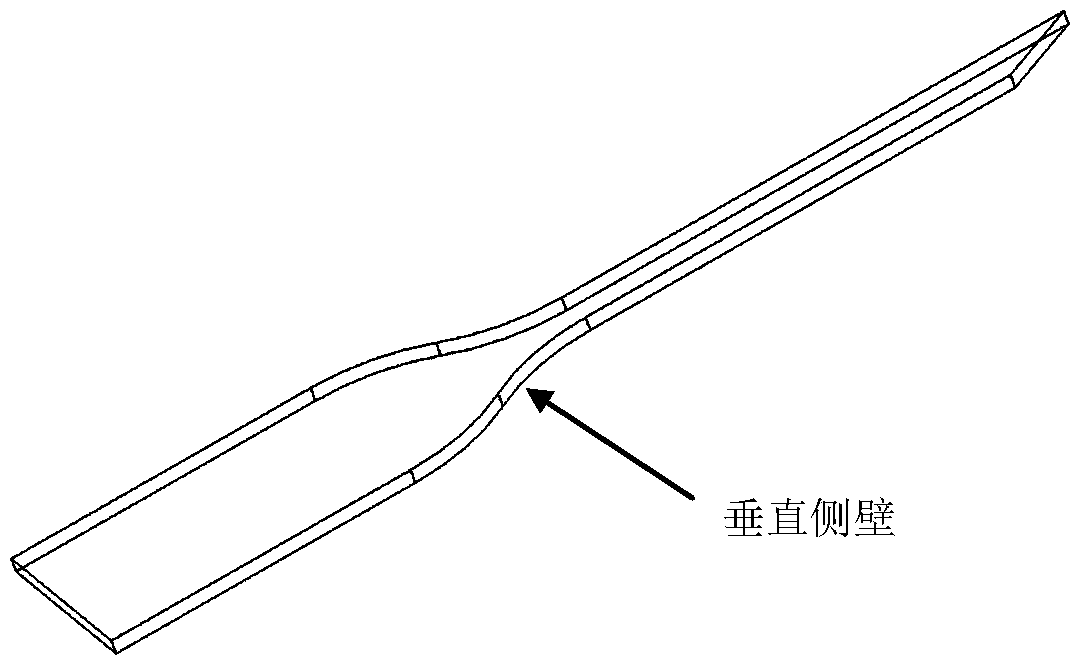
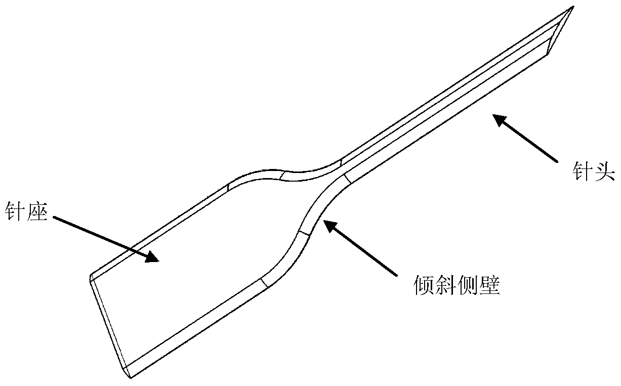
[0058] The prepared microneedle includes a needle head and a needle seat, and the side wall of the first layer of the needle head is vertical, such as figure 1 shown.
[0059] The first layer of vertical hollow metal microneedles on the side wall, the process is as follows:
[0060] Firstly, a glass sheet is selected as a substrate, and after cleaning, a chromium / copper seed layer is sputtered. Metal copper is electroplated on the seed layer as the release layer, the electroplating thickness is 1 μm, and the electroplating rate is 0.05 μm / min. Then cast a positive resist on the metal release layer, with a thickness of 10 μm, and use a mask to photoetch the first layer of microneedle structure patterns. Direct electroplating of metal nickel to fill the pattern to make the first layer of microneedles. The plating rate is 0.05 μm / min, and the plating thickness is 10 μm.
[0061] Then, the gold seed layer is sputtered, and the positive resist is shaken by 10 μm, and the channe...
Embodiment 2
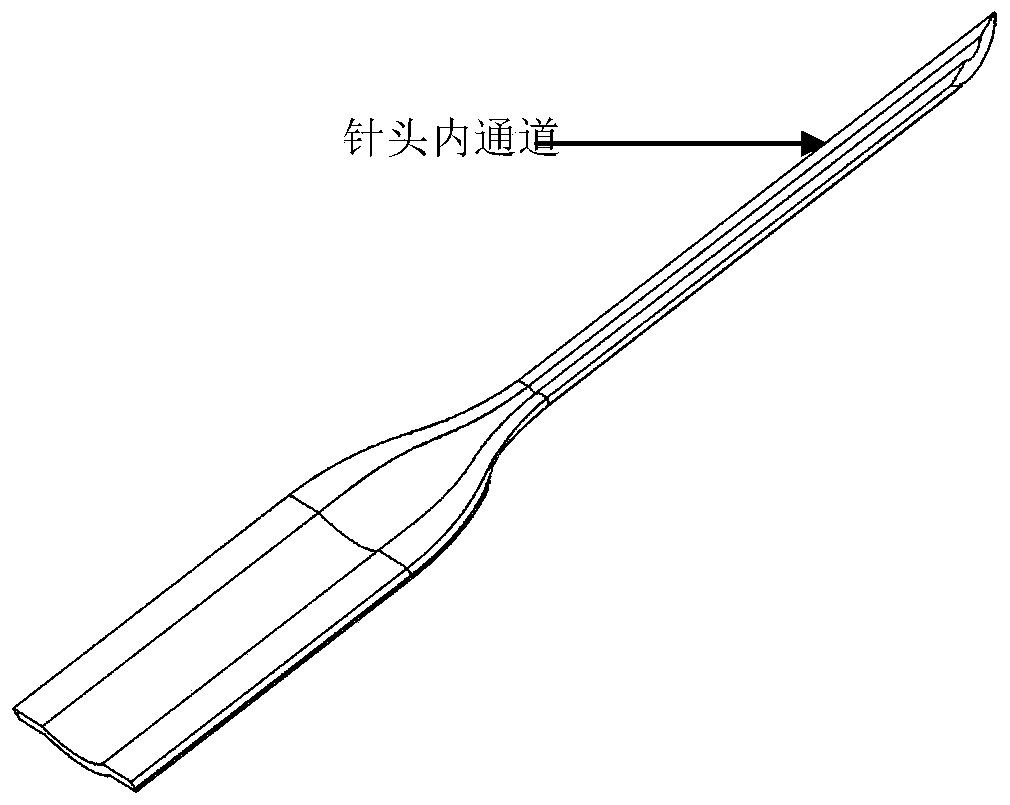
[0064] The prepared microneedle includes a needle head and a needle seat, and the section of the needle head is approximately elliptical, which is close to a traditional injection needle; the needle seat is convenient for connecting the microneedle with other parts, and at the same time enhances the strength of the microneedle.
[0065] The needle section is similar to the elliptical hollow metal microneedle, and the process is as follows:
[0066] The whole process is as Figure 6 As shown, a glass sheet 1 is first selected as a substrate, and after cleaning, a chromium / copper seed layer 2 is sputtered. Metal copper 3 is electroplated on the seed layer as a release layer, the electroplating thickness is 5 μm, and the electroplating rate is 0.2 μm / min. Then throw positive glue 4 on the metal release layer with a thickness of 50 μm, and use Figure 5 The mask 1 shown in the photocuts the pattern of the first layer structure of the microneedles. The patterned photoresist 4 is...
Embodiment 3
[0070] There is no needle seat, and the needle profile is similar to an elliptical hollow metal microneedle. The process is as follows:
[0071] Firstly, a glass sheet is selected as a substrate, and after cleaning, a chromium / copper seed layer is sputtered. Metal copper is electroplated on the seed layer as the release layer, the electroplating thickness is 20 μm, and the electroplating rate is 0.5 μm / min. Subsequently, positive resist was cast on the metal release layer with a thickness of 90 μm, and the structure pattern of the first layer of microneedles was photoetched using a needle-only mask. The patterned photoresist is programmed to bake to make the side wall of the pattern inclined and smooth, the heating rate is 1°C / min, and the maximum bake temperature is 90°C.
[0072] Electroplating metal nickel to fill the pattern to make the first layer of microneedles, the electroplating rate is 0.5 μm / min during electroplating, and the electroplating thickness is 90 μm. The...
PUM
| Property | Measurement | Unit |
|---|---|---|
| thickness | aaaaa | aaaaa |
| thickness | aaaaa | aaaaa |
| width | aaaaa | aaaaa |
Abstract
Description
Claims
Application Information


