Transverse IGBT (Insulated Gate Bipolar Translator) and manufacturing method therefor

A manufacturing method and horizontal technology, applied in semiconductor/solid-state device manufacturing, electrical components, circuits, etc., can solve problems such as IGBT characteristics deterioration, and achieve the effect of optimal electric field

Active Publication Date: 2015-09-02
GTA SEMICON CO LTD
View PDF3 Cites 0 Cited by
  • Summary
  • Abstract
  • Description
  • Claims
  • Application Information

AI Technical Summary

Problems solved by technology

[0005] The technical problem to be solved by the present invention is to overcome the defects in the prior art that the doping concentration distribution of the N-type buffer layer in the lateral IGBT is basically constant, which leads to the deterioration of the IGBT characteristics, and provide a kind of N-type buffer layer whose doping concentration distribution is a gradual type Transverse IGBT with more optimized electric field and better dynamic and static performance and its manufacturing method

Method used


Image

  • Transverse IGBT (Insulated Gate Bipolar Translator) and manufacturing method therefor
  • Transverse IGBT (Insulated Gate Bipolar Translator) and manufacturing method therefor
  • Transverse IGBT (Insulated Gate Bipolar Translator) and manufacturing method therefor

Examples


Embodiment 1

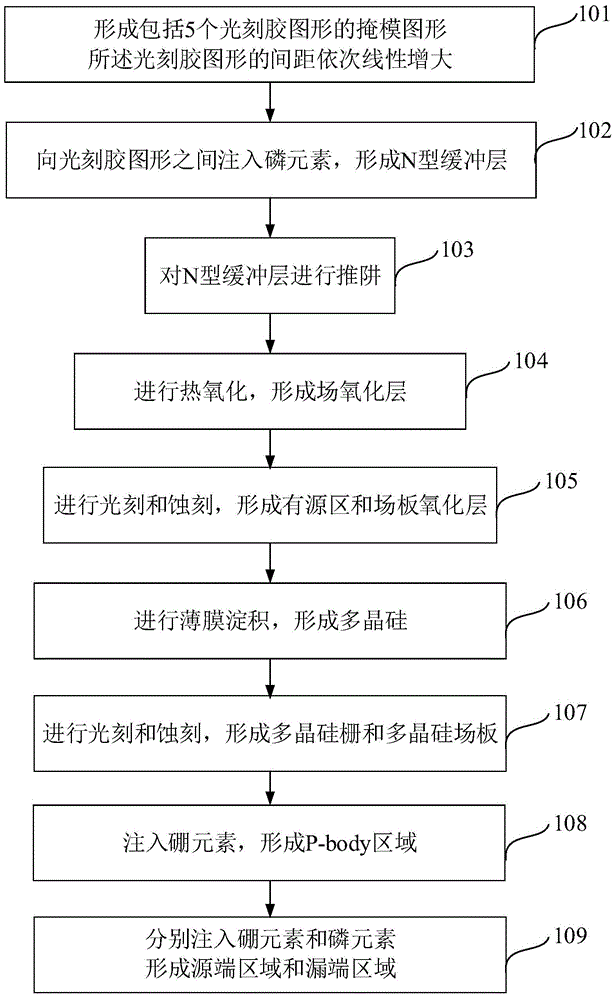
[0038] A method of making a horizontal IGBT, such as figure 1 shown, including the following steps:

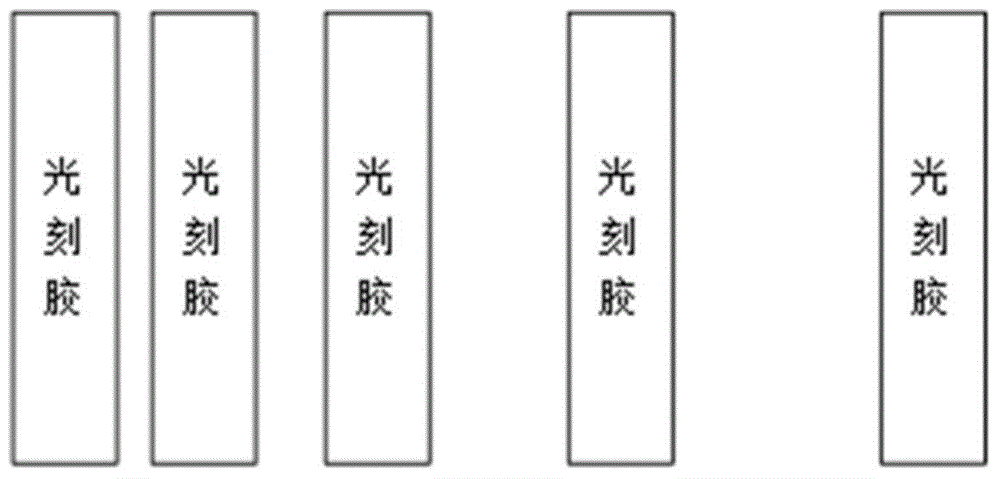
[0039] Step 101, forming a mask pattern, the mask pattern includes 5 photoresist patterns, such as figure 2 As shown, the pitch of the photoresist pattern increases linearly successively;

[0040] Step 102, injecting phosphorus elements between the photoresist patterns to form an N-type buffer layer;

[0041] Step 103, performing well pushing on the N-type buffer layer;

[0042] Step 104, performing thermal oxidation on a substrate to form a field oxide layer;

[0043] Step 105, performing photolithography and etching on the field oxide layer to form an active region and a field plate oxide layer;

[0044] Step 106, performing thin film deposition on the active region and the field plate oxide layer to form polysilicon;

[0045] Step 107, performing photolithography and etching on the polysilicon to form a polysilicon gate and a polysilicon field plate;

[0046] Step 10...

Embodiment 2

[0054] This embodiment provides a method for fabricating a lateral IGBT. The difference from the method of Embodiment 1 is that: in step 101, the length of the mask pattern is 100 microns, and the spacing of the photoresist pattern increases step by step; in step 102, Arsenic is injected between the photoresist patterns to form an N-type buffer layer; in step 109, boron and arsenic are injected respectively to form a source region and a drain region.

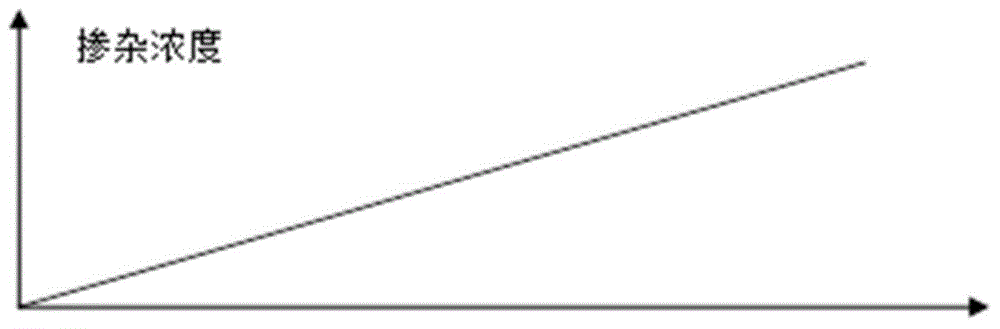
[0055] This embodiment also provides a 1200V lateral IGBT, which is manufactured by the above-mentioned manufacturing method, such as Figure 4 As shown, the doping concentration of the N-type buffer layer in the lateral IGBT is a stepwise distribution. Compared with the existing 1200V lateral IGBT, the lateral IGBT of this embodiment has better static characteristics, dynamic characteristics and switching characteristics.

[0056] It should be noted that the number and spacing of the photoresist patterns are determined by the ...


PUM


Abstract

The invention discloses a transverse IGBT (Insulated Gate Bipolar Translator) and a manufacturing method therefor. The manufacturing method comprises the following steps of S1, forming a mask pattern which comprises a plurality of photoresist images, wherein gaps among the photoresist images are gradually increased; and S2, injecting N-type doping among the photoresist images to form an N-type buffer layer. Compared with the manufacturing method of the conventional transverse IGBT, the manufacturing method provided by the invention is characterized in that the plurality of photoresist images with gradually-increasing gaps are arranged, the doping is injected into each gap, and the N-type buffer layer with gradually-changing doping density distribution is formed at a drain end of the IGBT, so that the IGBT device made by the manufacturing method provided by the invention has a better electric field characteristic, a better static state characteristic, a better dynamic characteristic, and a better switching characteristic.

Description

technical field [0001] The invention relates to the field of semiconductor devices, in particular to a lateral IGBT (Insulated Gate Bipolar Transistor, insulated gate bipolar transistor) and a manufacturing method thereof. Background technique [0002] IGBT is a new type of power semiconductor device, which has become a new generation of mainstream products in the field of power electronics. It integrates MOS gate control and bipolar conductance modulation to obtain high input impedance and low on-state resistance. It is currently the most ideal power switching devices. Among them, the basic structure of IGBT includes two types: horizontal type and vertical type. [0003] The development of vertical IGBT has gone through three generations of PT (Punch Through), NPT (Non Punch Through, non-punch through) and Field Stop (electric field stop). The Field Stop IGBT mainly forms an N-type buffer layer with a relatively light doping concentration on the back of the IGBT, which re...

Claims


Application Information

Patent Timeline
Patent Type & Authority Applications(China)
IPC IPC(8): H01L29/739H01L21/331H01L21/266H01L21/027
CPCH01L21/027H01L21/266H01L29/7393
Inventor 张栋
Owner GTA SEMICON CO LTD
Why Eureka
Try Eureka