Method and device for image detection of silicon wafer distribution state in semiconductor equipment carrying area

A technology of equipment carrying and distribution status, applied in image enhancement, image analysis, image data processing, etc., can solve problems such as damage to silicon wafers or equipment, collisions, missed reports, etc., to avoid damage to silicon wafers and equipment, and improve detection. Precision, good results

Active Publication Date: 2018-06-22
BEIJING NAURA MICROELECTRONICS EQUIP CO LTD
View PDF6 Cites 0 Cited by
  • Summary
  • Abstract
  • Description
  • Claims
  • Application Information

AI Technical Summary

Problems solved by technology

[0007] At present, the identification of the distribution state of the silicon wafers in the batch type silicon wafer heat treatment system generally adopts a simple photoelectric signal motion scanning method to identify the distribution state of the silicon wafers on the carrier 3. When the silicon wafer is in an abnormal state such as stacked wafers, inclined wafers or no wafers, it has a certain detection effect, but if the silicon wafer is in a protruding state on the carrier 3, it cannot be detected well, that is to say, by The existing technology simply obtains abnormal or normal results, but it is still easy to cause collisions during the motion scanning process, resulting in damage to the silicon wafer or equipment, and often produces false positives and false positives

Method used


Image

  • Method and device for image detection of silicon wafer distribution state in semiconductor equipment carrying area
  • Method and device for image detection of silicon wafer distribution state in semiconductor equipment carrying area
  • Method and device for image detection of silicon wafer distribution state in semiconductor equipment carrying area

Examples


Embodiment 1

[0162] In this embodiment, two photoelectric sensors / or ultrasonic sensor solutions on the machine are adopted; the implementation of step S3 in this kind of solution may specifically include the following steps (taking photoelectric sensors 4 and 5 as examples):

[0163] Step S31: According to the thickness of the silicon wafer and the distance between adjacent silicon wafers, obtain the motion scanning area for judging the oblique slice, laminated slice and empty slice;

[0164] Step S32: Manipulator 1 is positioned at the position of the end point of the horizontal movement and the position of the vertical start point;

[0165] Step S33: According to the preset detection area where the two photoelectric sensors 4, 5 transmit and receive light signals and the light signal shielding width in this area, sequentially determine whether there are oblique slices, stacked slices and / or the corresponding silicon wafer placement positions Or the abnormal state of empty sheet; If yes,...

Embodiment 2

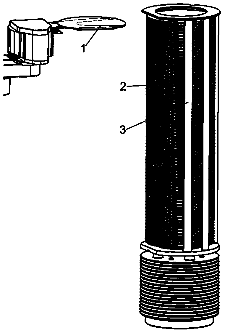
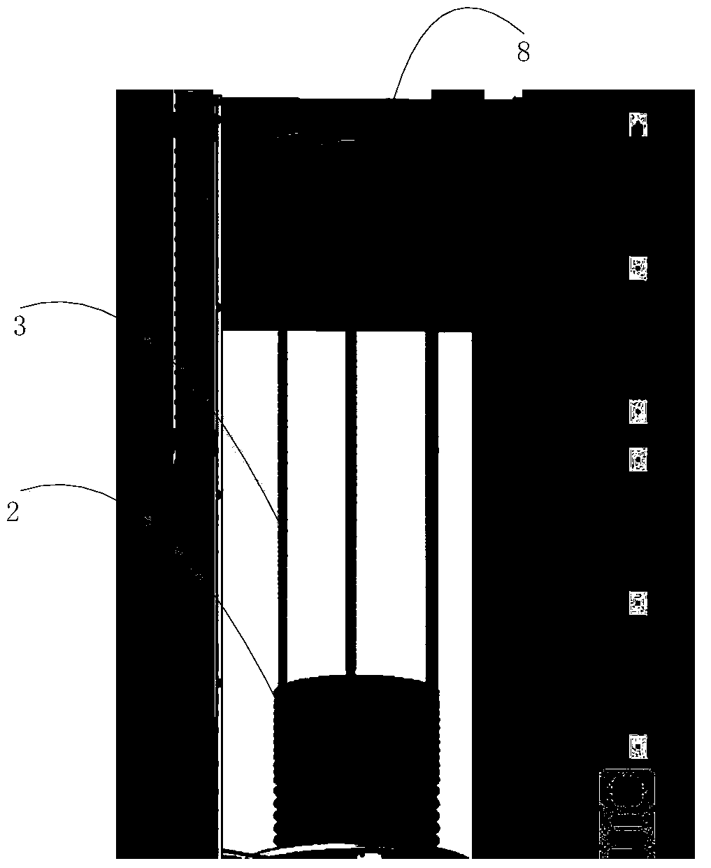
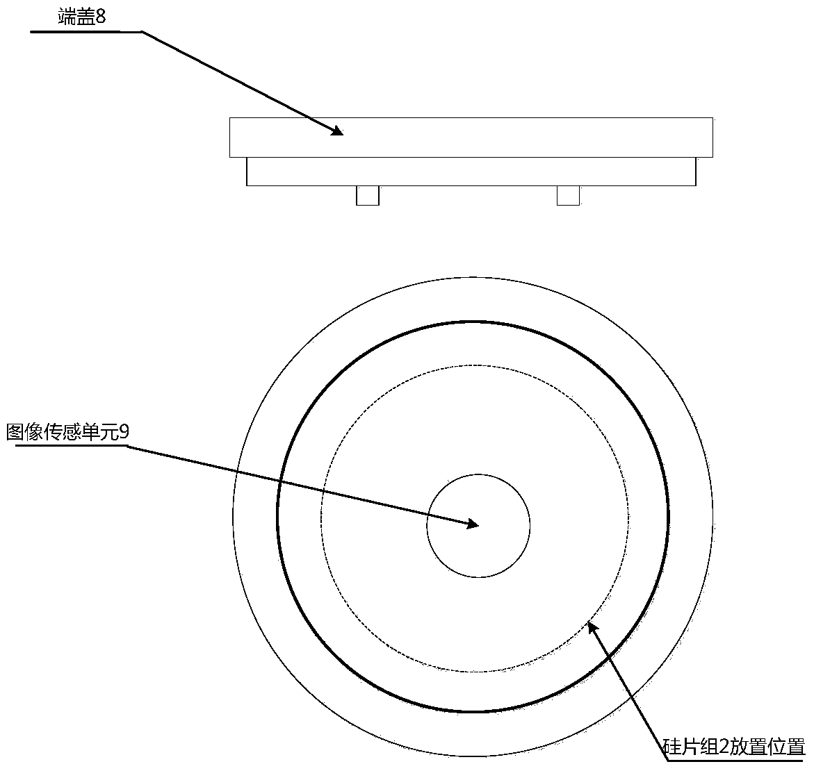
[0189] In the embodiment of the present invention, if the image sensing unit in the image detection device for the distribution state of the silicon wafer in the semiconductor equipment carrying area is located on the manipulator, then, in the embodiment of the present invention, the image sensing unit is used in the The scheme of collecting the side graphics of each silicon wafer in the silicon wafer group 2 can also be used to determine whether there is an abnormal state of oblique wafers, stacked wafers and / or empty wafers. The implementation of step S3 of the scheme can specifically include the following steps :

[0190] Step S31': According to the thickness of the silicon wafer, the distance between adjacent silicon wafers and the thickness of the carrier, obtain the motion scanning area for judging the inclined wafer, laminated wafer and empty wafer;

[0191] Step S32': Manipulator 1 is positioned at the starting point of the horizontal motion and the vertical end point;...


PUM


Abstract

The invention provides a method and device of detecting silicon chip distribution status images within a semiconductor equipment load bearing region. An image sensing unit is arranged above a silicon chip group; an optoelectronic scanning unit or an ultrasonic scanning unit is arranged on an opposite position of a mechanical arm U-shaped end portion on the periphery of a silicon chip bearing device; the silicon chip bearing device and the mechanical arm can perform relative rotation and / or positioning motion. In an image capture mode of a first detection phase, executing a command to pre-scan abnormal state extreme positions of bulge plates of silicon chips; in a mutual receiving mode of the optoelectronic scanning / ultrasonic scanning unit in a second detection phase, executing a command to scan round abnormal states of bulge plates of silicon chips; and in a mutual receiving mode of the optoelectronic scanning / ultrasonic scanning unit in a third detection phase, executing a command to scan silicon chip distribution state abnormity. A plurality of scanning detection points are set on the periphery of the silicon chip bearing device, thereby further improving detection accuracy.

Description

technical field [0001] 本发明涉及半导体加工设备技术领域,尤其涉及一种半导体设备承载区域的硅片分布状态图像检测方法,本发明还涉及一种半导体设备承载区域的硅片分布状态图像检测装置。 Background technique [0002] 硅片的安全存取和输运是集成电路大生产线一个非常重要的技术指标,在生产过程中,通常要求由于输运设备自身导致的硅片破片率应小于十万分之一。并且,作为批量式硅片热处理系统,相对于单片式工艺系统,每个生产工艺所需的硅片传输、硅片放置和取片次数更多,因而对硅片传输、硅片放置和取片的安全性和可靠性要求更高。 [0003] 目前,机械手被广泛应用于半导体集成电路制造技术领域中,机械手是硅片传输系统中的重要设备,用于存取和输运工艺处理前和工艺处理后的硅片,其能够接受指令,精确地定位到三维或二维空间上的某一点进行取放硅片,既可对单枚硅片进行取放作业,也可对多枚硅片进行取放作业。 [0004] 然而,当机械手在对硅片进行取放作业时,尤其是,当硅片在传输过程或热处理过程中导致的受热变形等情况会导致硅片在承载器上处于突出状态或者处于叠片、斜片或无片状态时,往往会产生碰撞导致硅片或设备受损,造成不可弥补的损失。 [0005] see figure 1 , figure 1 为现有技术中机械手在硅片传输、硅片放置和取片时的位置结构示意图。如图所示,当硅片组2中的硅片在承载器3上处于突出等异常状态时,机械手1在自动存取硅片2的运动处于非完全工作状态,非常容易造成硅片2及设备(包括机械手1)的损伤。 [0006] 因此,在机械手1完成硅片放置后或准备取片前,需对承载器3上硅片组2中的硅片分布状态进行准确的识别,同时对识别出的各种异常状态提供准确应对措施,以实现安全取放片。 [0007] 目前,批量式硅片热处理系统的硅片分布状态的识别一般是采用单纯的光电信号运动扫描方法对硅片在承载器3上的分布状态进行识别,这种扫描方法仅对硅片组2中的硅片处于叠片、斜片或无片等异常状态时,有一定的检测效果,但如果硅片在承载器3上处于突出状态时,就不能很好地检测出,也就是说,通过现有技术简单的得出异常或正常的结果,在运动扫描过程中还是易产生碰撞导致硅片或设备受损,同时经常产生漏报、误报的情况。 [0008...

Claims


Application Information

Patent Timeline
Patent Type & Authority Patents(China)
IPC IPC(8): G06T7/00
CPCG06T7/0004G06T2207/10052G06T2207/10132G06T2207/30148
Inventor 徐冬
Owner BEIJING NAURA MICROELECTRONICS EQUIP CO LTD
Why Eureka
Try Eureka