Touch control display device, manufacturing method thereof and electronic equipment

A touch display device and touch electrode technology, which is applied to circuits, electrical components, electrical digital data processing, etc., can solve the problems of long production cycle, large process error, complicated preparation process, etc., and achieve low production cost and process error. The effect of small size and simple preparation process

Active Publication Date: 2015-09-16
WUHAN CHINA STAR OPTOELECTRONICS TECH CO LTD
View PDF3 Cites 24 Cited by
  • Summary
  • Abstract
  • Description
  • Claims
  • Application Information

AI Technical Summary

Problems solved by technology

Therefore, the preparation process of the above-mentioned fully embedded touch displa

Method used


Image

  • Touch control display device, manufacturing method thereof and electronic equipment
  • Touch control display device, manufacturing method thereof and electronic equipment
  • Touch control display device, manufacturing method thereof and electronic equipment

Examples


Example Embodiment

[0042] The implementation of the present invention will be described in detail below in conjunction with the accompanying drawings and examples, so as to fully understand and implement the process of how to apply technical means to solve technical problems and achieve technical effects in the present invention. It should be noted that, as long as there is no conflict, each embodiment and each feature in each embodiment of the present invention can be combined with each other, and the formed technical solutions are all within the protection scope of the present invention.

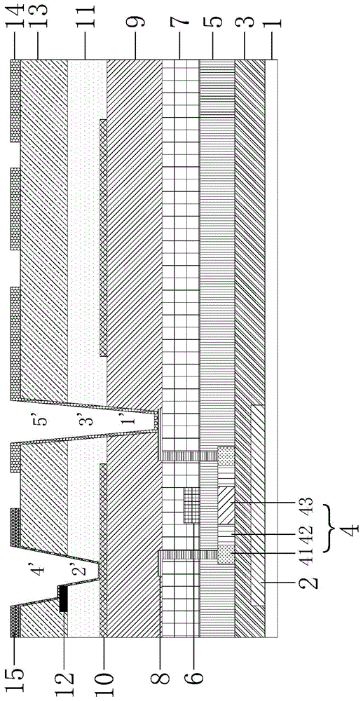
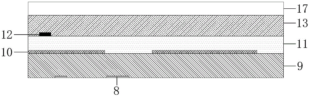
[0043] The technical problem to be solved by the present invention is: when preparing the fully embedded touch display device in the prior art, the formation of the via hole 1 used to connect the touch electrode and the common electrode, and the via hole 1 used to connect the pixel electrode and the thin film The formation of via hole 2, via hole 3 and via hole 4 of the metal layer of the data line of the tra...


PUM


Abstract

The invention discloses a touch control display device, a manufacturing method thereof and electronic equipment. When the touch control display device is manufactured, a via hole enabling a connecting electrode to be connected with a touch control electrode and a common electrode and a via hole enabling a pixel electrode to be connected with a data line metal layer can be formed through one photolithographic process. Manufacturing technology is simple, technological error is small, production period is short, production cost is low, and production efficiency is improved greatly.

Description

technical field [0001] The present invention relates to the field of display technology, in particular to a touch display device, a method for preparing the touch display device and electronic equipment with the touch display device. Background technique [0002] With the development of touch technology, full in-cell touch (Full In-Cell Touch) display devices are more and more widely used. The fully embedded touch display device in the current technology includes a thin film transistor (TFT, Thin Film Transistor), a flat layer (PLN layer), a common electrode, an interface layer (IL layer), a touch electrode, a protective layer, and pixels arranged in sequence. electrode. Specifically, the touch electrodes are connected to the common electrodes through via holes opened on the interface layer. The pixel electrode is sequentially connected to the data line metal layer of the thin film transistor through via hole 2 formed on the protection layer, via hole 3 formed on the inter...

Claims


Application Information

Patent Timeline
IPC IPC(8): G06F3/041H01L21/768
Inventor 陈归薛景峰
Owner WUHAN CHINA STAR OPTOELECTRONICS TECH CO LTD
Why Eureka
Try Eureka