Package structure and package method for high definition LED display screen module

A technology for LED display and module packaging, applied in the direction of identification devices, instruments, electrical components, etc., can solve the problem of not meeting the requirements of high-definition LED display, and achieve the effect of reasonable packaging structure layout, reasonable layout and cost reduction.

Inactive Publication Date: 2015-09-16
安徽国晶微电子有限公司
View PDF8 Cites 4 Cited by
  • Summary
  • Abstract
  • Description
  • Claims
  • Application Information

AI Technical Summary

Problems solved by technology

With the development of science and technology and economy, the market has higher and higher requirements for the clarity of the display screen, and now the mainstream LED display manufacturers adopt the chip technology to manufacture the LED display pixel pitch with a minimum

Method used


Image

  • Package structure and package method for high definition LED display screen module
  • Package structure and package method for high definition LED display screen module
  • Package structure and package method for high definition LED display screen module

Examples


Embodiment Construction

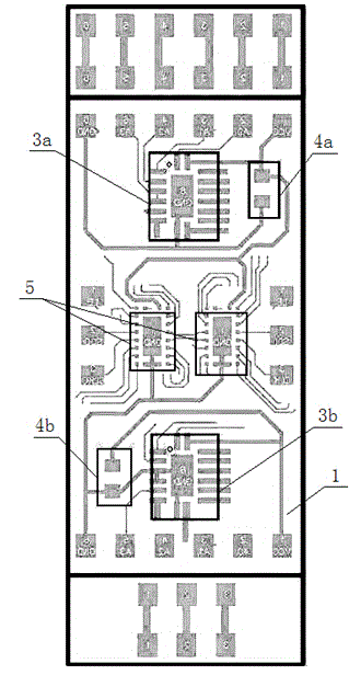
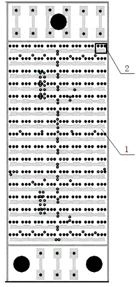
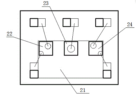
[0029] See figure 1 and figure 2 , high-definition LED display module packaging structure, including a PCB board 1, 128 pixel units 2 connected to the front of the PCB board 1 and arranged in a determinant (8x16), two QFN circuits 3a connected to the back of the PCB board 1, 3b, two capacitors 4a, 4b and two driver IC chips 5, the LED potting adhesive layer coated on the surface of 128 pixel units 2 and the vinyl layer coated on the surface of the driver IC chip 5; the adjacent two The distance between the centers of the pixel units 2 is 1.5mm; two driver IC chips 5 are connected to the middle of the back of the PCB board 1, two QFN circuits 3a, 3b and two capacitors 4a, 4b are divided into two groups, respectively located in the two driver ICs Above and below the chip 5, that is, one of the QFN circuits 3a and one capacitor 4a are located above the two driver IC chips 5, and the other QFN circuit 3b and another capacitor 4b are located below the two driver IC chips 5;

[0...


PUM


Abstract

The invention discloses a package structure and a package method for a high definition LED display screen module. The package structure for the high definition LED display screen module comprises a PCB, a plurality of pixel units, QFN circuits, capacitors and driving IC chips, wherein the pixel units are connected to the front face of the PCB and arranged in a determinant mode, the QFN circuits, the capacitors and the driving IC chips are connected to the back face of the PCB, and the central distance between every two adjacent pixel units is 1.5mm. The integral structure of the package structure meets the requirement of the market for the definition of the high definition LED display screen. The package structure is reasonable in layout and high in package precision, the packaged LED display screen module is wide in application range, and the LED display screen module can be used for large screen display of an indoor instruction dispatch system and high definition display of a film screen.

Description

technical field [0001] The invention relates to the field of LED display screens, in particular to a high-definition LED display screen module packaging structure and packaging method. Background technique [0002] LED display developed rapidly in the world in the late 1980s and became a new type of display media. It uses dot matrix pixel units composed of light-emitting diodes to form a large-area display screen. It has high reliability, long service life, strong environmental adaptability, and high cost performance. With the characteristics of low cost of use, it has rapidly grown into one of the mainstream products of flat panel display in just two decades, and has been widely used in the field of information display. With the development of science and technology and economy, the market has higher and higher requirements for the clarity of the display screen, and now the mainstream LED display manufacturers adopt the chip technology to manufacture the LED display pix...

Claims


Application Information

Patent Timeline
IPC IPC(8): G09F9/33H01L25/075H01L33/48
CPCG09F9/33H01L25/0753H01L33/48
Inventor 王士勇庞士德史少峰
Owner 安徽国晶微电子有限公司
Why Eureka
Try Eureka