Low-temperature polycrystalline silicon thin film, manufacturing method thereof and related device

A low-temperature polysilicon and thin-film technology, applied in the direction of electric solid-state devices, semiconductor devices, polycrystalline material growth, etc., can solve the problems of insufficient mobility and affecting the performance of thin-film transistors, etc.

Active Publication Date: 2015-09-23
BOE TECH GRP CO LTD
View PDF3 Cites 13 Cited by
  • Summary
  • Abstract
  • Description
  • Claims
  • Application Information

AI Technical Summary

Problems solved by technology

[0004] Embodiments of the present invention provide a low-temperature polysilicon thin film, its manufacturing method, and related devices, to solve the problem in th...

Method used


Image

  • Low-temperature polycrystalline silicon thin film, manufacturing method thereof and related device
  • Low-temperature polycrystalline silicon thin film, manufacturing method thereof and related device
  • Low-temperature polycrystalline silicon thin film, manufacturing method thereof and related device

Examples


Embodiment Construction

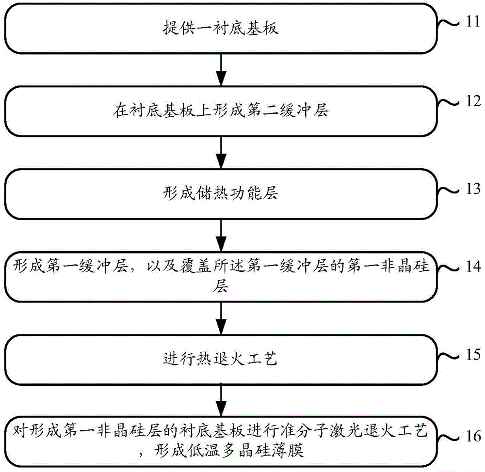
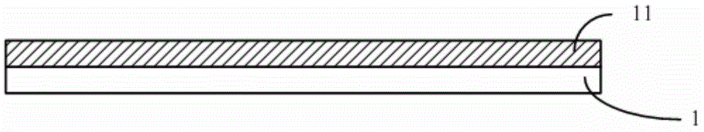
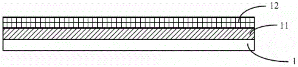
[0028] In order to make the purpose, technical solutions and advantages of the present invention clearer, the present invention will be further described in detail below in conjunction with the accompanying drawings. Obviously, the described embodiments are only some of the embodiments of the present invention, rather than all of them. Based on the embodiments of the present invention, all other embodiments obtained by persons of ordinary skill in the art without making creative efforts belong to the protection scope of the present invention.

[0029] In the embodiment of the present invention, by forming the heat storage functional layer on the base substrate and separating it from the amorphous silicon layer on the surface by the buffer layer, when the excimer laser annealing process is performed, the non-crystalline silicon layer on the surface The crystalline silicon layer can use the energy released by the underlying heat storage functional layer to delay the cooling time,...


PUM

PropertyMeasurementUnit
Thicknessaaaaaaaaaa
Thicknessaaaaaaaaaa

Abstract

The invention discloses a low-temperature polycrystalline silicon thin film, a manufacturing method thereof and a related device. The method mainly comprises the steps of providing an underlayment substrate, forming a heat storage function layer on the underlayment substrate, forming a first buffer layer on the heat storage function layer, forming a first amorphous silicon layer to cover the first buffer layer, and conducting the excimer laser annealing treatment on the underlayment substrate provided with the first amorphous silicon layer to form a low-temperature polycrystalline silicon film. The heat storage function layer and the first amorphous silicon layer can be in the heat absorption state at the same time, and can also be in the heat radiation state at the same time. Therefore, during the excimer laser annealing treatment, the cooling duration is prolonged by the first amorphous silicon layer on the surface of the polycrystalline silicon thin film, based on the utilization of the heat storage function layer at the bottom of the polycrystalline silicon thin film. In this way, the growth duration of low-temperature polysilicon is prolonged, and the grain size of low-temperature polysilicon is increased.

Description

technical field [0001] The invention relates to the field of display technology, in particular to a low-temperature polysilicon thin film, a manufacturing method thereof, and related devices. Background technique [0002] OLED display panels made of low-temperature polysilicon have display advantages such as ultra-thin, low power consumption, and self-luminescence. Therefore, a new generation of organic light-emitting diode OLED display panels derived from low-temperature polysilicon LTPS has become an important technical branch of current display technology. . [0003] At present, the most important factor affecting the performance of OLED display panels is the mobility of low-temperature polysilicon. Compared with amorphous silicon, low-temperature polysilicon has advantages such as greater mobility and higher stability; As far as the industry is concerned, its mobility still cannot well meet the current development needs. Therefore, it is necessary to obtain low-temperat...

Claims


Application Information

Patent Timeline
IPC IPC(8): H01L21/77H01L29/786H01L27/32
CPCH10K59/125H01L21/0245H01L21/02488H01L21/02502H01L21/0262H01L29/78603H01L21/02532H01L21/02686H01L29/6675H01L29/78672C30B1/023C30B28/02C30B29/06H01L21/02592H01L27/1222H01L27/1285H01L29/78696
Inventor 徐文清田宏伟龙春平
Owner BOE TECH GRP CO LTD
Why Eureka
Try Eureka