Substrate integrated waveguide ferrite tunable band-pass filter

A substrate-integrated waveguide and ferrite technology, applied in waveguide-type devices, electrical components, circuits, etc., can solve the problems of low feasibility, signal interference, poor electromagnetic compatibility, etc., and achieve easy planarization and integration, The effect of large power capacity and easier integration

Inactive Publication Date: 2015-09-23
UNIV OF ELECTRONICS SCI & TECH OF CHINA
View PDF7 Cites 9 Cited by
  • Summary
  • Abstract
  • Description
  • Claims
  • Application Information

AI Technical Summary

Problems solved by technology

Although this structure realizes the adjustable frequency of the filter, it requires the joint control of DC bias and voltage, that is, the combination of electric control and magnetic control, the structure is complex, and because the substrate integrated waveguide is an equipotential body, the bias voltage cannot be directly applied , requires additional separate circuitry to implement voltage control
[0005] Literature "Magnetically Tunable Ferrite-Loaded Half-Mode Substrate Integrated Waveguide" (S.Adhikari, S.Hemour, A.Ghiotto, and K.Wu, IEEE Micro.Wireless Comp. Lett., vol.25, no.3, pp .172-174, March 2015." Publication of substrate-integrated waveguide tunable band-pass filter uses ferrite and lumped capacitors loaded on half-mode substrate-integrated waveguide to realize band-pass filter bandwidth adjustable, but there are the following problems : 1) The half-mode substrate integrated waveguide filter is a semi-open structure, which is easily interfered by other signals in the circuit and has poor electromagnetic compatibility; 2) It only realizes the adjustable bandwidth, and does not realize the adjustment of the operating frequency under the same bandwidth; 3) The adjustment of the capacitance value needs to replace the capacitor, which is not feasible in actual use
[0006] At present, there is no suitable solution for the design of ferrite-loaded tunable bandpass filter based on substrate integrated waveguide

Method used


Image

  • Substrate integrated waveguide ferrite tunable band-pass filter
  • Substrate integrated waveguide ferrite tunable band-pass filter
  • Substrate integrated waveguide ferrite tunable band-pass filter

Examples


Embodiment 1

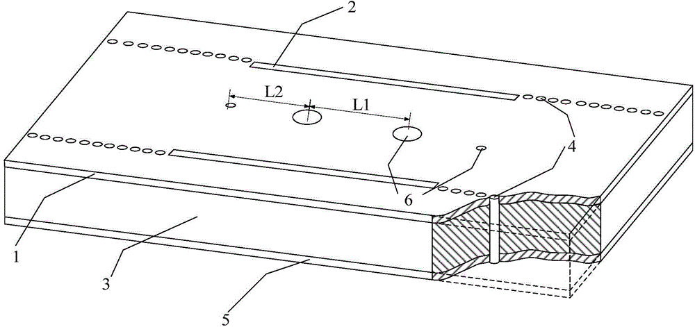
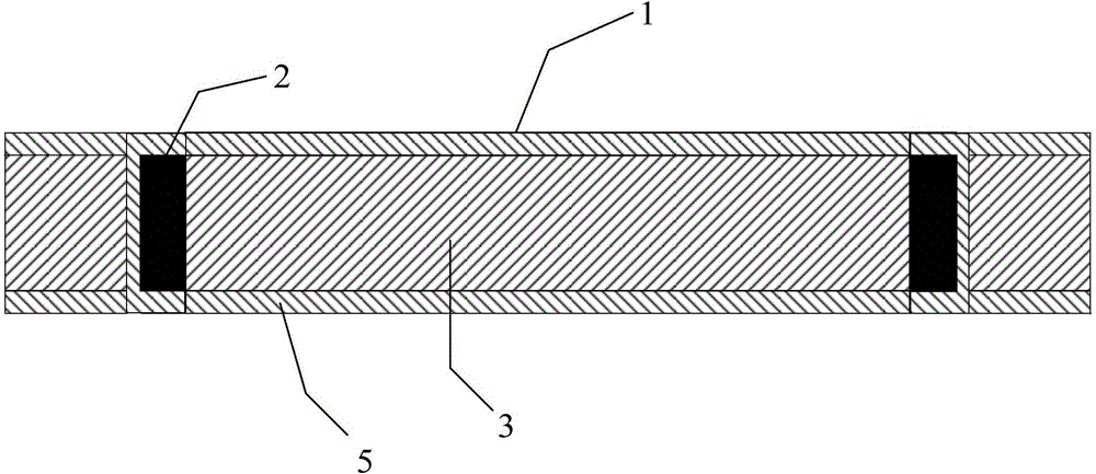
[0031] Such as figure 1 , figure 2 As shown, the substrate-integrated waveguide ferrite tunable bandpass filter in this embodiment includes metallized copper-clad upper layer 1 and ferrite metallized on three sides (near the outer side and upper and lower surfaces of the narrow edge of the substrate-integrated waveguide). Body block 2, dielectric substrate 3, narrow-side metallized through hole 4, metal copper-clad lower layer 5, central inductive metallized through-hole 6; the substrate integrated waveguide consists of metal copper-clad upper layer 1 and metal copper-clad lower layer 5 through two rows of mutual The parallel narrow-side metallized through holes 4 are connected together and constituted together with the corresponding dielectric substrate 3; the center of the substrate integrated waveguide dielectric layer 3 is the central inductive metallized through hole 6, and the two sides of the dielectric substrate 3 are embedded with three-sided metallized ferrite bloc...

Embodiment 2

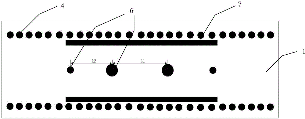
[0034] Such as image 3 , Figure 4 As shown, in this embodiment, the substrate-integrated waveguide ferrite tunable bandpass filter includes a metal-clad copper upper layer 1, a ferrite block 7 metallized on the upper and lower surfaces, a dielectric substrate 3, and narrow-side metallized Through hole 4, metal copper-clad lower layer 5, central inductive metallized through hole 6; the substrate integrated waveguide is connected by metal copper-clad upper layer 1 and metal copper-clad lower layer 5 through two rows of metallized through-holes 4 parallel to each other, and corresponding The dielectric substrate 3 is formed together; the center of the substrate integrated waveguide dielectric layer 3 is a central inductive metallization through hole 6, and the two sides of the substrate integrated waveguide are embedded with metallized ferrite blocks 7 on the upper and lower surfaces, and the outside of the ferrite block 7 If the processing technology allows, it should be as c...


PUM

PropertyMeasurementUnit
thicknessaaaaaaaaaa
widthaaaaaaaaaa
lengthaaaaaaaaaa

Abstract

The invention belongs to the technical field of tunable filters, and relates to a substrate integrated waveguide ferrite tunable band-pass filter. The substrate integrated waveguide ferrite tunable band-pass filter comprises an upper metal copper coating layer, a dielectric layer, a narrow-edge metalized through holes, a lower metal copper coating layer and central inductive metallized through holes, wherein the lower metal copper coating layer is sequentially provided with the dielectric substrate and the upper metal copper coating layer, the upper metal copper coating layer and the lower metal copper coating layer are connected through two rows of mutually parallel narrow-edge metallized through holes, and the upper metal copper coating layer and the lower metal copper coating layer form a substrate integrated waveguide together with the dielectric layer; and the center of the substrate integrated waveguide is provided with a row of central inductive metalized through holes. The substrate integrated waveguide ferrite tunable band-pass filter is characterized in that the dielectric layer is provided with ferrite blocks in an embedded mode at positions close to the two rows of narrow-edge metallized through holes, and the upper surface and the lower surface of each ferrite block are metallized and respectively connected with the upper metal copper coating layer and the lower metal copper coating layer in a conduction mode. According to the invention, the ferrite loaded substrate integrated waveguide tunable band-pass filter is realized so as to meet requirements for the tunable band-pass filter in a substrate integrated system.

Description

technical field [0001] The invention belongs to the technical field of adjustable filters, in particular to a ferrite adjustable band-pass filter based on substrate integrated waveguide technology. Background technique [0002] The concept of substrate integrated circuits based on ordinary printed circuit board (PCB) technology has been greatly developed since it was proposed in 2000, and the most concerned one is substrate integrated waveguide technology. In recent years, on the basis of sufficient research on the transmission characteristics of substrate integrated waveguide structures, magnetron devices such as ferrite tunable filters based on substrate integrated waveguide technology have been realized, which has greatly promoted the development of substrate integrated waveguide technology. new development. Currently, reconfigurability and miniaturization are the main development directions of filters. [0003] The traditional waveguide tunable bandpass filter is large...

Claims


Application Information

Patent Timeline
Patent Type & Authority Applications(China)
IPC IPC(8): H01P1/203
Inventor 程钰间黄秋栋刘小亮宣志杰
Owner UNIV OF ELECTRONICS SCI & TECH OF CHINA
Why Eureka
Try Eureka