Integrated device for seamed butt joint of AWG (arrayed waveguide grating) output waveguide and detector and preparation method

An output waveguide and integrated device technology, applied in the field of optoelectronic devices and their integration, can solve the problems of high coupling energy consumption, poor system stability, affecting applications, etc., and achieve high coupling efficiency, improve lateral alignment accuracy, and improve stability. Effect

Active Publication Date: 2015-09-30
INST OF SEMICONDUCTORS - CHINESE ACAD OF SCI
View PDF4 Cites 9 Cited by
  • Summary
  • Abstract
  • Description
  • Claims
  • Application Information

AI Technical Summary

Problems solved by technology

[0004] In the process of realizing the present invention, the applicant found that in the prior art, the AWG output waveguide and the waveguide detector are set separately, the stability of the system is poor, and the coupling energy consumption is high, which affects the application of the two in the field of optical communication.

Method used


Image

  • Integrated device for seamed butt joint of AWG (arrayed waveguide grating) output waveguide and detector and preparation method
  • Integrated device for seamed butt joint of AWG (arrayed waveguide grating) output waveguide and detector and preparation method
  • Integrated device for seamed butt joint of AWG (arrayed waveguide grating) output waveguide and detector and preparation method

Examples


Embodiment Construction

[0033] In the present invention, the main structure of the device is constructed by semiconductor technology, and the compatibility of the AWG and the epitaxial structure of the waveguide detector is realized through the secondary epitaxy technology. The presence of can improve the yield of the device.

[0034] In order to make the object, technical solution and advantages of the present invention clearer, the present invention will be described in further detail below in conjunction with specific embodiments and with reference to the accompanying drawings.

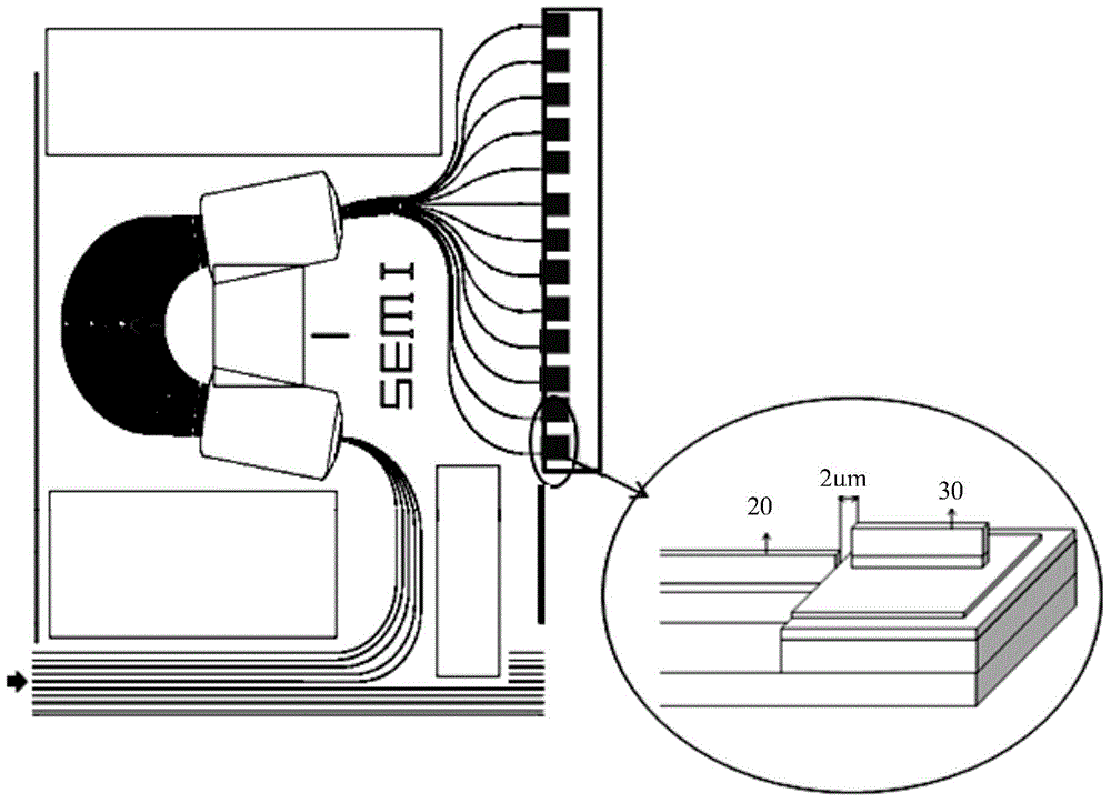
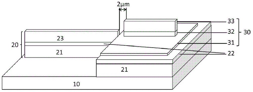
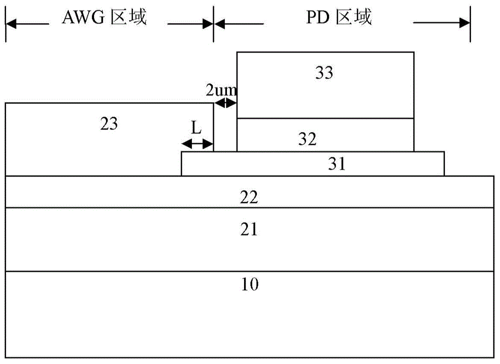
[0035] In an exemplary embodiment of the present invention, an integrated device in which an AWG output waveguide and a waveguide detector are slotted butted is provided. Figure 1A It is a three-dimensional view of an integrated device in which an AWG output waveguide and a waveguide detector are jointed with a slot according to an embodiment of the present invention. Figure 1B for Figure 1A The cross-sectional view of...


PUM


Abstract

The invention provides an integrated device for seamed butt joint of an AWG (arrayed waveguide grating) output waveguide and a waveguide photodetector and a preparation method of the integrated device. The integrated device comprises a substrate, the AWG output waveguide and the waveguide photodetector, wherein the left area and the right area of the substrate are taken as an AWG area and a PD (photodetector) area respectively; the AWG output waveguide is located on the AWG area on the substrate, and an AWG lower coating layer and an AWG core layer extend to the PD area; the waveguide photodetector is formed above the AWG core layer in the PD area on the substrate, and a PD lower contact layer of the waveguide photodetector extends into an AWG upper coating layer of the AWG output waveguide and is located above the AWG core layer; a PD absorbing layer and a PD upper contact layer of the waveguide photodetector are spaced with the AWG upper coating layer of the AWG output waveguide by a narrow seam. According to the integrated device and the preparation method, excessive coupling loss generated during interconnection of discrete devices is avoided, and the energy efficiency of an optical link is improved through evanescent field coupling; meanwhile, by means of the seam between the AWG output waveguide and the waveguide photodetector, the capacitance of PD devices is reduced, and the device bandwidth is increased.

Description

technical field [0001] The invention relates to the field of optoelectronic devices and their integration, in particular to an integrated device in which an AWG output waveguide and a waveguide detector are connected with a slot and a preparation method thereof. Background technique [0002] The emergence of various information networks covering the whole world marks the entry of human beings into the information society. With the development of society, people's demand for information services is increasing day by day, and correspondingly, the bandwidth of the communication system is required to increase continuously. In order to meet the increasing transmission traffic in the world, the process of intelligent optical network characterized by all-optical information processing and information service broadband represented by fiber-to-the-home is accelerating. A new generation of optical fiber communication evolution with integration, low cost and high reliability. The wav...

Claims


Application Information

Patent Timeline
Patent Type & Authority Applications(China)
IPC IPC(8): G02B6/12G02B6/13
CPCG02B6/12009G02B6/131G02B6/136
Inventor 吕倩倩韩勤杨晓红尹伟红
Owner INST OF SEMICONDUCTORS - CHINESE ACAD OF SCI
Why Eureka
Try Eureka