Plasma processing device and electrostatic chuck thereof and manufacturing method of electrostatic chuck

A processing device and plasma technology, applied in semiconductor/solid-state device manufacturing, circuits, discharge tubes, etc., can solve the problem of uneven temperature distribution of electrostatic chucks, difficult electrostatic chuck temperature uniformity, and uneven heating of electrostatic chucks And other issues

Active Publication Date: 2015-09-30
ADVANCED MICRO FAB EQUIP INC CHINA
View PDF4 Cites 9 Cited by
  • Summary
  • Abstract
  • Description
  • Claims
  • Application Information

AI Technical Summary

Problems solved by technology

[0004] In the prior art, due to the large area of ​​the electrostatic chuck, it is difficult to ensure the uniformity of the temperature in each area of ​​the electrostatic chuck while the electrostatic chuck is rapidly heating up, and the temperature in different areas will have obvious differences and even form cold areas. And the hot zone, resulting in uneven heating of the substrate by the electrostatic chu...

Method used


Image

  • Plasma processing device and electrostatic chuck thereof and manufacturing method of electrostatic chuck
  • Plasma processing device and electrostatic chuck thereof and manufacturing method of electrostatic chuck
  • Plasma processing device and electrostatic chuck thereof and manufacturing method of electrostatic chuck

Examples


Embodiment Construction

[0039] The specific embodiment of the present invention will be further described in detail below in conjunction with the accompanying drawings.

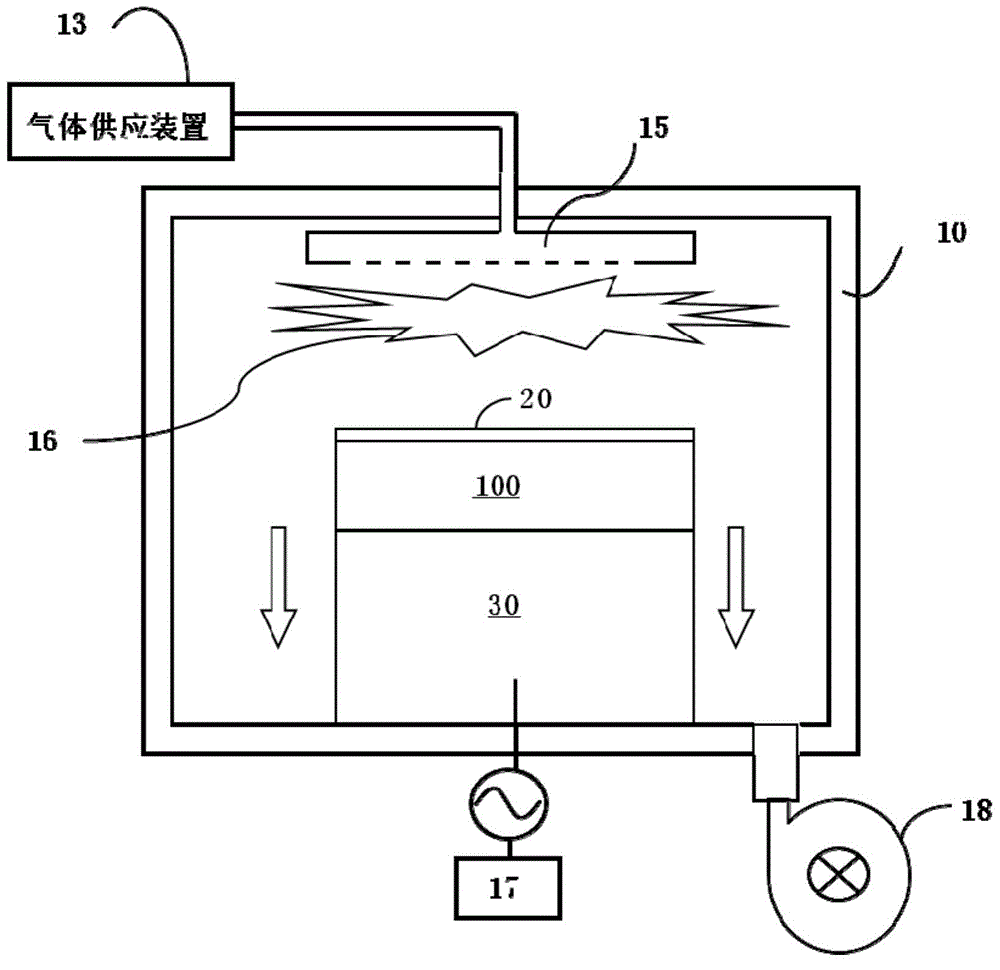
[0040] The technical scheme described in the invention is applicable to capacitively coupled plasma reaction chambers or inductively coupled plasma reaction chambers, as well as other plasma reaction chambers that use electrostatic chucks to support substrates to be processed. Exemplary, figure 1A schematic diagram of the structure of the plasma reaction chamber of the present invention is shown; the plasma reaction chamber is a capacitively coupled plasma reaction chamber, and any deformations made by those skilled in the art through the technical solutions disclosed in the present invention without creative labor belong to protection scope of the present invention.

[0041] figure 1 A schematic diagram of the structure of a plasma reaction chamber is shown, including a roughly cylindrical reaction chamber 10, and upper and lower...


PUM


Abstract

The invention provides a plasma processing device and an electrostatic chuck thereof and a manufacturing method of the electrostatic chuck. The electrostatic chuck comprises a metal pedestal. Heating devices are arranged on the metal pedestal. Heat-conducting plates are arranged on the heating devices. Ceramic insulating layers are arranged on the heat-conducting plates. Height of the heating devices to a substrate and height of the heat-conducting plates to the substrate are different, and heat-conducting adhesive layers with controllable thickness are arranged between the ceramic insulating layers and the heat-conducting plates so that uniform surface temperature of the ceramic insulating layers or multi-parameter adjustment with specific temperature gradient can be realized. Power supply power of the heating devices can be adjusted, and adjustment of surface temperature of the ceramic insulating layers can be also realized by adjusting height difference of the heating devices of different heating areas, thickness of the heat-conducting plates of different heat areas and thickness of the heat-conducting adhesive layers between the ceramic insulating layers and the heat-conducting plates so that temperature controllability of the electrostatic chuck can be greatly increased, and rapid adjustment of temperature uniformity or specific gradient of different areas of the electrostatic chuck is facilitated.

Description

technical field [0001] The invention relates to a semiconductor processing technology, and more specifically, relates to the technical field of an electrostatic chuck. Background technique [0002] In the process of plasma etching or chemical vapor deposition, etc., an Electro Static Chuck (ESC) is often used to fix, support and transport the substrate (Wafer) waiting to be processed. The electrostatic chuck is set in the reaction chamber, which uses electrostatic attraction instead of mechanical means to fix the substrate, which can reduce the possible mechanical loss of the substrate, and make the electrostatic chuck and the substrate completely contact, which is conducive to heat conduction . [0003] Existing electrostatic chucks usually include an insulating layer, a heating layer, and a metal base supporting the insulating layer and the heating layer, and a DC electrode is arranged in the insulating layer, and the electrostatic attraction is applied to the substrate a...

Claims


Application Information

Patent Timeline
IPC IPC(8): H01L21/683H01J37/32
Inventor 何乃明吴狄倪图强
Owner ADVANCED MICRO FAB EQUIP INC CHINA
Why Eureka
Try Eureka