Interconnect structure and method of forming the same

A technology of interconnect structure and dielectric layer, which is applied in the manufacturing of electrical components, electric solid-state devices, semiconductor/solid-state devices, etc., can solve the problem of decreased quality and reliability of interconnect structures, increased etching rate, and conductive plug overhang, etc. The problem is to prevent the undercut phenomenon between the interfaces, improve the quality and reliability, and eliminate the existence of the interface.

Active Publication Date: 2018-03-30
SEMICON MFG INT (SHANGHAI) CORP
View PDF3 Cites 0 Cited by
  • Summary
  • Abstract
  • Description
  • Claims
  • Application Information

AI Technical Summary

Problems solved by technology

[0009] However, during the formation of the conductive plug 160, the conductive plug 160 at the interface between the first low-K dielectric layer 110 and the protective layer 120 will form an overhang phenomenon. The reason for the overhang phenomenon is: in the laminated structure (including the first low-K dielectric layer 110 , the protection layer 120 and the hard mask layer 130 ), after forming the through hole, it is necessary to use an acid solution to pickle the through hole; during the pickling process, the acid solution A low-K dielectric layer 110, the protection layer 120 and the hard mask layer 130 all have a certain etching effect, and the etching rates of the first low-K dielectric layer 110, the protection layer 120 and the hard mask layer 130 are sequentially increased by the acid solution , after cleaning, the widths of the through holes in the first low-K dielectric layer 110, the protective layer 120 and the hard mask layer 130 increase sequentially, that is, a bottom appears at the junction of the protective layer and the first low-K dielectric layer. The undercut phenomenon, in fact, also occurs at the junction of the hard mask layer 130 and the protective layer 120; this undercut phenomenon leads to the formation of conductive plugs when the via holes are filled with conductive materials. overhang
[0010] The overhang phenomenon causes voids to appear in the interlayer dielectric layer near the conductive plug during the formation of the conductive plug, resulting in a decrease in the quality and reliability of the interconnection structure
[0011] For this reason, a new method of forming an interconnection structure is needed to prevent the conductive plugs from protruding during the formation of the interconnection structure, thereby preventing holes in the interlayer dielectric layer near the conductive plugs, thereby preventing the interconnection structure from forming. The quality and reliability of the

Method used


Image

  • Interconnect structure and method of forming the same
  • Interconnect structure and method of forming the same
  • Interconnect structure and method of forming the same

Examples


Embodiment Construction

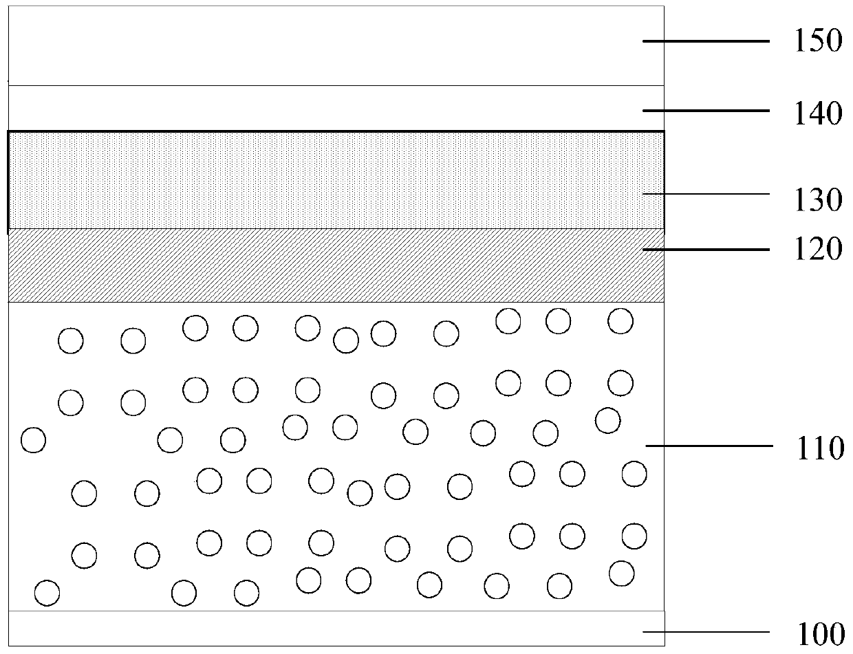
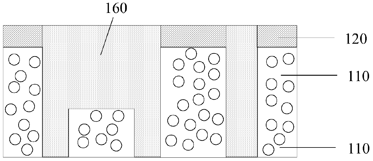
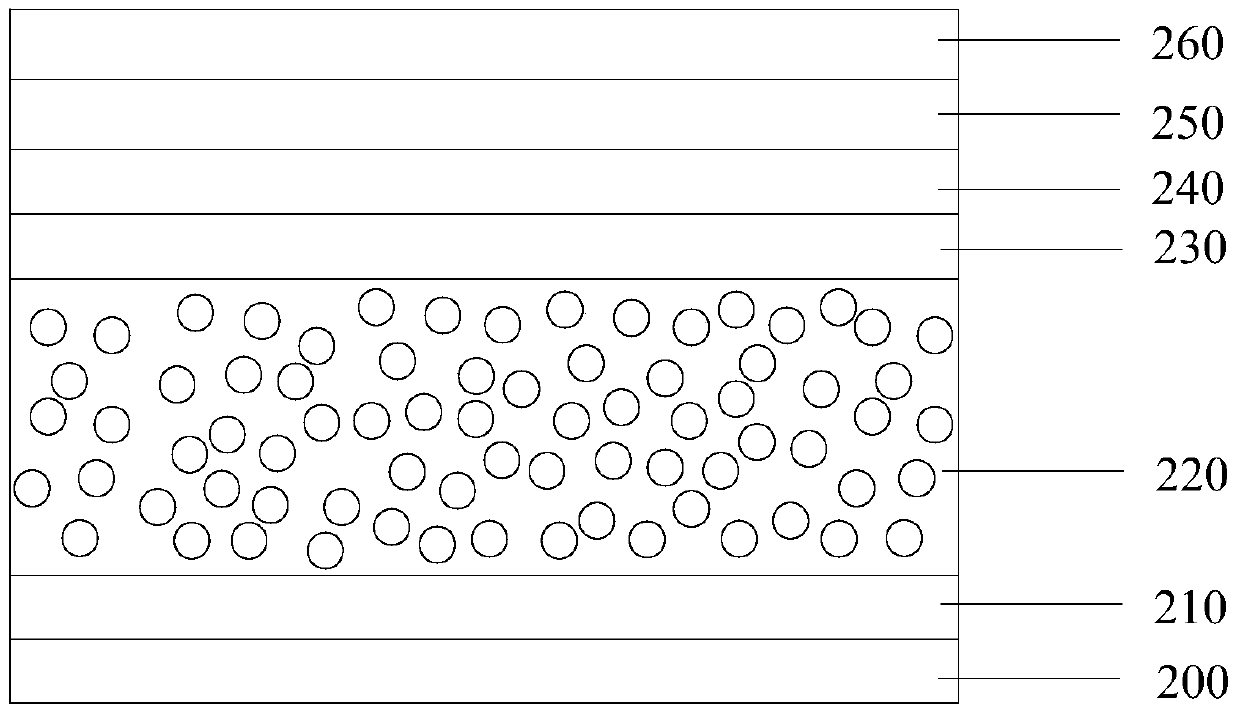
[0039] As described in the background art, during the formation process of the existing interconnect structure, there is a problem that the conductive plugs are prone to overhang in each stacked structure, resulting in the formation of the conductive plugs, the interlayer dielectric near the conductive plugs The layers are highly prone to voids, which degrade the quality and reliability of the interconnect structure.

[0040] The present invention provides a new interconnection structure and a method for forming the same. The forming method forms a dense dielectric layer on the ultra-low K dielectric layer. The dense dielectric layer itself has a protective function, so it is not necessary to form the protective layer, and then the dense dielectric layer is formed on the dense dielectric layer. A mask layer is formed on the layer, and then the mask layer, the dense dielectric layer and the ultra-low K dielectric layer are sequentially etched from top to bottom until through hol...


PUM


Abstract

An interconnection structure and a method for forming the same. Wherein, the forming method of the interconnection structure includes: providing a substrate; forming an ultra-low K dielectric layer on the substrate; forming a dense dielectric layer on the ultra-low K dielectric layer; forming a mask on the dense dielectric layer film layer; sequentially etching the mask layer, dense dielectric layer and ultra-low K dielectric layer from top to bottom until a through hole is formed; filling the through hole with a conductive material to form a conductive plug. The forming method improves the quality and reliability of the finally formed interconnection structure, and the forming method has simple process, saves process steps and saves cost.

Description

technical field [0001] The present invention relates to the field of semiconductor manufacturing, and in particular, to an interconnection structure and a method for forming the same. Background technique [0002] Currently, in the back-end process of semiconductor manufacturing, in order to connect various components to form an integrated circuit, it is usually necessary to fabricate an interconnection structure. Among interconnect structures, structures used to connect active regions of semiconductor devices with other integrated circuits are generally conductive plugs. Existing conductive plugs are usually formed by a via process or a dual damascene process. [0003] In the formation process of the existing interconnect structure, through holes are formed by etching a low-K dielectric layer, and then conductive plugs are formed by filling conductive materials in the through holes. However, when the feature size is below the deep sub-micron process, in order to prevent t...

Claims


Application Information

Patent Timeline
Patent Type & Authority Patents(China)
IPC IPC(8): H01L21/768H01L23/532
Inventor 周鸣
Owner SEMICON MFG INT (SHANGHAI) CORP
Why Eureka
Try Eureka