A process method for chemical mechanical planarization of devices with a size below 40nm

A chemical-mechanical and process technology, applied in semiconductor/solid-state device manufacturing, electrical components, circuits, etc., can solve problems such as circuit failure yield, affect device performance, and decrease, and achieve the goal of reducing metal loss and improving performance and yield. Effect

Active Publication Date: 2019-06-14
INST OF MICROELECTRONICS CHINESE ACAD OF SCI
View PDF6 Cites 0 Cited by
  • Summary
  • Abstract
  • Description
  • Claims
  • Application Information

AI Technical Summary

Problems solved by technology

[0005] However, under the current process conditions, the material removal rate of W formed by ALD is much higher than that of W formed by CVD, so that a large metal loss (Disshing / Loss) will be caused on the top of the metal gate. Affect device performance, even cause circuit failure and yield reduction

Method used


Image

  • A process method for chemical mechanical planarization of devices with a size below 40nm
  • A process method for chemical mechanical planarization of devices with a size below 40nm
  • A process method for chemical mechanical planarization of devices with a size below 40nm

Examples


Embodiment Construction

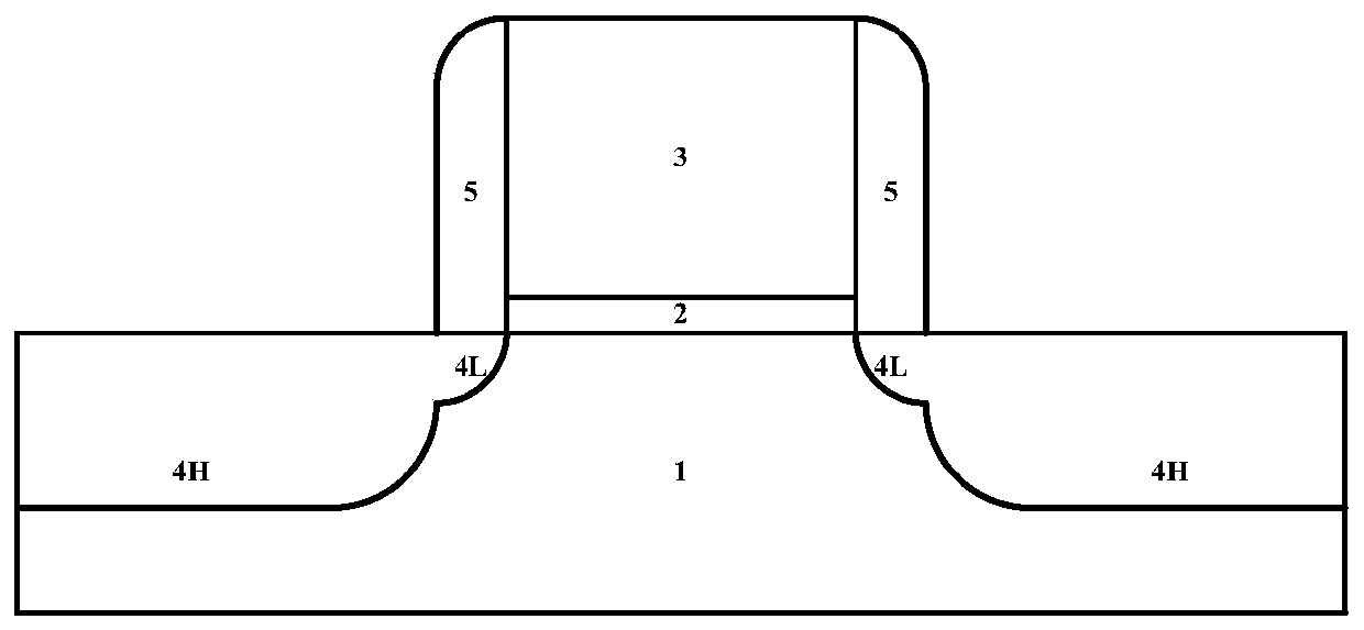
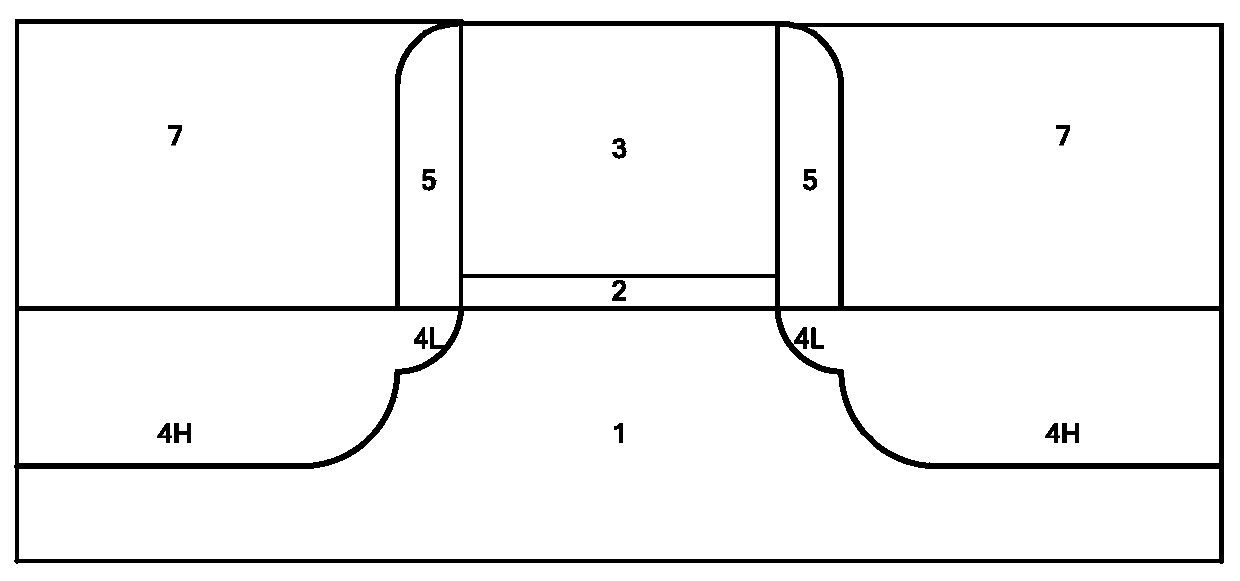
[0025] Embodiments of the present invention are described in detail below, examples of which are shown in the drawings, wherein the same or similar reference numerals designate the same or similar elements or elements having the same or similar functions throughout. The embodiments described below by referring to the figures are exemplary only for explaining the present invention and should not be construed as limiting the present invention.

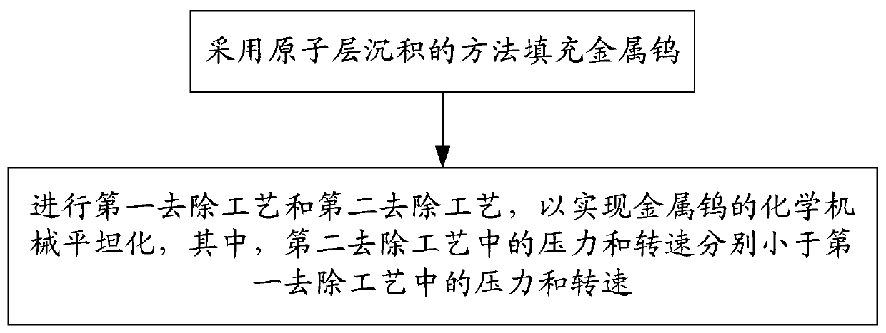
[0026] In the present invention, in the planarization process of the ALD metal tungsten, the problem that the removal rate is too high causes great loss of other layers. For this, as figure 1 Shown, the present invention proposes following technical scheme:

[0027] Metal tungsten is filled by atomic layer deposition;

[0028] A first removal process and a second removal process are performed to achieve chemical mechanical planarization of metal tungsten, wherein the pressure and rotation speed in the second removal process are respect...


PUM


Abstract

The invention provides a chemical machinery planarization process method. The method comprises the following steps: filling metallic tungsten by use of an atomic layer deposition method; carrying out a first removal process and a second removal process so as to realize chemical machinery planarization of the metallic tungsten, wherein the pressure and the rotating speed in the second removal process are respectively smaller than the pressure and the rotating speed in the first removal process. According to the invention, the chemical machinery planarization of the metallic tungsten is realized by use of a two-step removal process, and the pressure and the rotating speed in the later removal process are reduced, such that the mechanical effect in a grinding process is reduced in the second removal process, metal loss at the top of a metal gate can be reduced, and the performance and the yield of a device are improved.

Description

technical field [0001] The invention relates to the field of semiconductor manufacturing, in particular to a process method for chemical mechanical planarization of devices with a size below 40nm. Background technique [0002] At present, the gate-last process is currently widely used in the manufacture of advanced integrated circuit processes. It usually forms the dummy gate and source and drain regions first, then removes the dummy gate and refills the replacement gate of the high-k metal gate stack in the gate trench. . Since the gate is formed after the source and drain, the gate does not need to withstand a high annealing temperature in this process, and the selection of gate layer materials is wider and can better reflect the intrinsic characteristics of the material. [0003] In the prior art, conventional methods such as chemical vapor deposition (CVD) and physical vapor deposition (PVD) are often used to prepare metals such as Al and Mo as the metal filling layer f...

Claims


Application Information

Patent Timeline
Patent Type & Authority Patents(China)
IPC IPC(8): H01L21/768H01L21/321
Inventor 杨涛卢一泓张月崔虎山赵超李俊峰
Owner INST OF MICROELECTRONICS CHINESE ACAD OF SCI
Why Eureka
Try Eureka