Method for press fitting thick copper printed circuit board

A printed circuit board, thick copper technology, applied in the direction of circuit lamination, printed circuit, printed circuit manufacturing, etc., can solve the problems of weak withstand voltage, high cost, pressing and filling pressing voids, etc., to avoid voltage withstand Decrease in capacity, enhance filling effect, alleviate the effect of pressing voids

Inactive Publication Date: 2015-10-28
SHENZHEN SUNTAK MULTILAYER PCB
View PDF4 Cites 13 Cited by
  • Summary
  • Abstract
  • Description
  • Claims
  • Application Information

AI Technical Summary

Problems solved by technology

[0005] For this reason, the technical problem to be solved by the present invention is to overcome the technical bottleneck of the existing printed circuit board production process, which is prone to lamination voids due to poor lamination and filling, resulting in weaker voltage withstand capability and frequent breakdown of the product. , and the existing solutions have problems of high cost and low efficiency, so a lamination method for thick copper printed circuit boards is proposed

Method used


Image

  • Method for press fitting thick copper printed circuit board
  • Method for press fitting thick copper printed circuit board
  • Method for press fitting thick copper printed circuit board

Examples


Embodiment

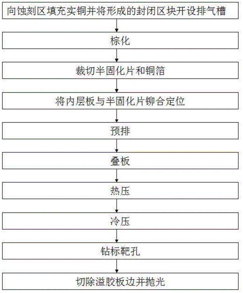
[0033] The invention provides a lamination method of a thick copper printed circuit board, such as figure 1 shown, including the following steps:

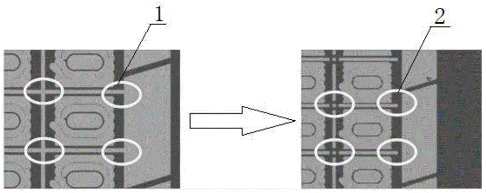
[0034] (1) if figure 2 As shown, the etched area of ​​the inner layer board of the printed circuit board is filled with solid copper. Before filling the solid copper, the residual copper rate of the etched area is 63%, and the residual copper rate of the etched area reaches 73%. The closed block 1 formed after being filled with solid copper is provided with an exhaust groove 2, and the width of the exhaust groove 2 is 25-30mm;

[0035] (2) browning, the inner layer board is oxidized, and an oxide layer is formed on the surface of the inner layer board, specifically: entering the board according to the order → sticking dust → using Na with a concentration of 20g / L 2 S 2 o 8 and 30ml / L H 2 SO 4 Acid washing and micro-etching to remove oxides and oil stains on the surface of the inner layer board → washing the inner layer board...


PUM


Abstract

The invention belongs to the field of circuit board processing and discloses a method for press fitting a thick copper printed circuit board. The method comprises the following steps of: filling an etched area of the inner-layer board of the printed circuit board with copper and arranging an air discharge duct on an enclosed block formed by filling the copper; performing brown oxide; cutting a prepreg and a copper foil and riveting the inner-layer board and the prepreg by using rivets in an overlapped manner to achieve laminated positoning; prearranging the inner-layer board; stacking boards; performing hot pressing and cold pressing treatment; and drilling a mark hole. After the etched area is filled with the copper, the residual copper rate of the inner-layer board is at least increased by 5 to 10%. Thus, the filling effect of the inner-layer board is obviously enhanced; a technology problem of press fit cavities is effectively relieved, and a decrease in the voltage withstand capability of a product is prevented. The air discharge duct arranged after the copper is filled guarantees good flow of the prepreg in a press fitting production process.

Description

technical field [0001] The invention belongs to the field of circuit board processing, and in particular relates to a pressing method for thick copper printed circuit boards. Background technique [0002] With the rapid development of electronic information technology, users are increasingly demanding printed circuit boards such as high-power and high-current server power boards, and these printed circuit boards need to have high heat resistance and high heat dissipation, so they generally need to be designed For thick copper plate. In the manufacturing process of multi-layer thick copper printed circuit boards, lamination is an essential process, which usually refers to the use of prepregs to bond the inner circuit board and the inner circuit board, and the inner circuit board under high temperature and high pressure conditions. Bonding with copper foil to make a multilayer circuit board. Among them, the prepreg refers to a sheet-like bonding material synthesized by resin...

Claims


Application Information

Patent Timeline
Patent Type & Authority Applications(China)
IPC IPC(8): H05K3/46
CPCH05K3/4632H05K2203/06H05K2203/14
Inventor 宋建远白会斌敖四超王淑怡
Owner SHENZHEN SUNTAK MULTILAYER PCB
Why Eureka
Try Eureka