
Manufacturing method of superconducting conductor and superconducting conductor

A manufacturing method and technology of superconducting conductors, applied in the usage of superconducting elements, cable/conductor manufacturing, superconducting/high-conducting conductors, etc., to achieve the effect of good superconducting properties

Active Publication Date: 2017-10-13
FURUKAWA ELECTRIC CO LTD
View PDF5 Cites 0 Cited by
  • Summary
  • Abstract
  • Description
  • Claims
  • Application Information

AI Technical Summary

Problems solved by technology

On the other hand, the superconducting wire obtained by forming an intermediate layer and a superconducting layer on a metal substrate wider than the desired width may be further thinned.

Method used


Image

  • Manufacturing method of superconducting conductor and superconducting conductor
  • Manufacturing method of superconducting conductor and superconducting conductor
  • Manufacturing method of superconducting conductor and superconducting conductor

Examples


no. 1 Embodiment approach

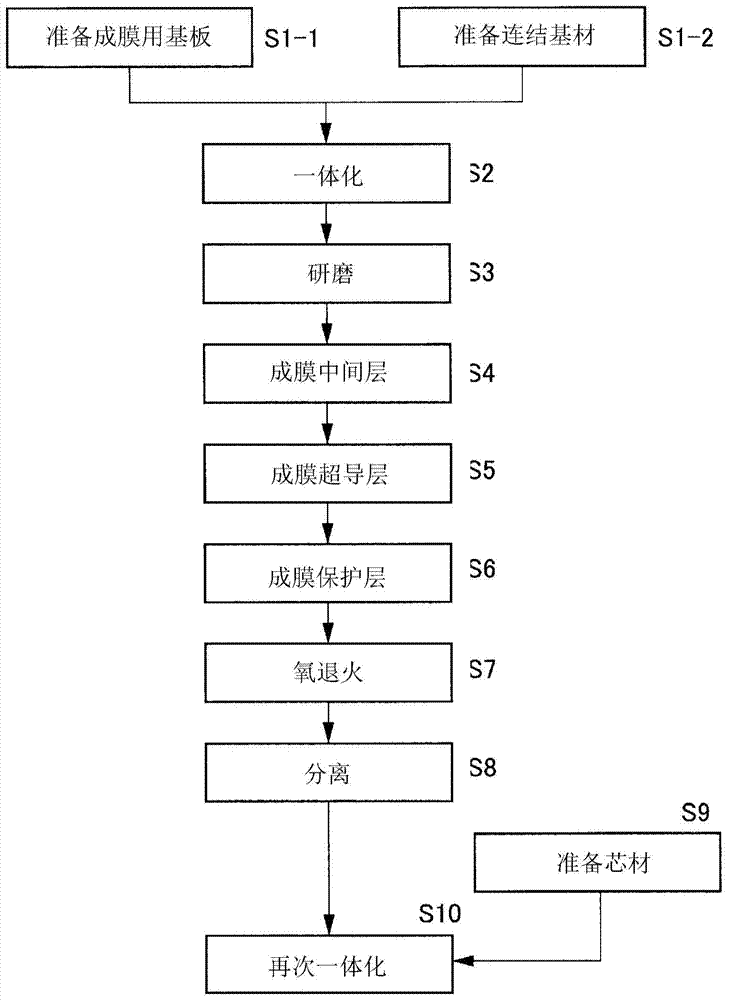
[0030] As a first embodiment of the present invention, a method in which a plurality of narrow film-forming substrates are embedded in a joint base material to be integrated, and an intermediate layer, a superconducting layer, After performing oxygen annealing on the protective layer, the superconducting wires are produced in units of film-forming substrates by separating them from the connecting substrates, and the obtained superconducting wires are wound around the outer circumference of the circular core wires and again Integrate to produce a circular composite superconducting conductor. figure 1 It is a flowchart of the main process.

[0031]

[0032] Form the wire to the specified cross-sectional dimensions. The metal used is preferably a material having a Vickers hardness (Hv hardness: VIckers-hardness) greater than 100, and alloys containing Cu, Ni, Ti, Mo, Nb, Ta, W, Fe, and Ag can be used. Particularly preferred are stainless steel, Hastelloy (registered trademark...

Embodiment 1

[0089] Examples 1 to 4 according to the above-mentioned first embodiment will be described.

[0090] (Example 1)

[0091] In Example 1, a plurality of superconducting wires having a narrow film-forming substrate having a thickness of t0.05 mm x a width of w1.0 mm produced through the steps described in the first embodiment were produced, and the obtained superconducting wires were used. The wire yields a circular composite superconducting conductor.

[0092]

[0093] will diameter The metal wire (round wire) of Hastelloy C276 was formed into a shape of thickness t0.05mm×width w1.0mm×length L1050m at a processing rate of about 34%.

[0094]

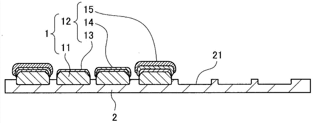
[0095] Ten grooves of depth d0.03mm×width w1.0mm are formed in parallel at a pitch of 2.5mm in the width direction over the entire length of the Hastelloy C276 alloy bar of t0.15mm×w26.5mm×L105m, and become Connect the substrate.

[0096]

[0097] The narrow film-forming substrate was inserted into ten grooves formed in the join...

Embodiment 2

[0120] In Example 2, a plurality of superconducting wires having a narrow film-forming substrate having a thickness t0.1 mm×width w2.00 mm were produced through the steps described in the first embodiment. Here, only steps S1-1, S1-2 and S2 will be described. The other steps (S3 to S8) are omitted because they are the same as those in Example 1.

[0121]

[0122] will diameter The metal wire (round wire) of Hastelloy C276 was formed into a shape of thickness t0.1mm×width w2.0mm×length L740m at a processing rate of about 34%.

[0123]

[0124] Seven grooves of depth d0.08mm x width w2.0mm are formed in parallel at a pitch of 3.5mm in the width direction over the entire length of the Hastelloy C276 alloy bar of thickness t0.2mm x width w26.5mm x length L105m , and become the connecting substrate.

[0125]

[0126] The narrow film-forming substrate was inserted into seven grooves formed in the joint base material, and the narrow film-forming substrate and the joint base...


PUM

PropertyMeasurementUnit
surface roughnessaaaaaaaaaa

Abstract

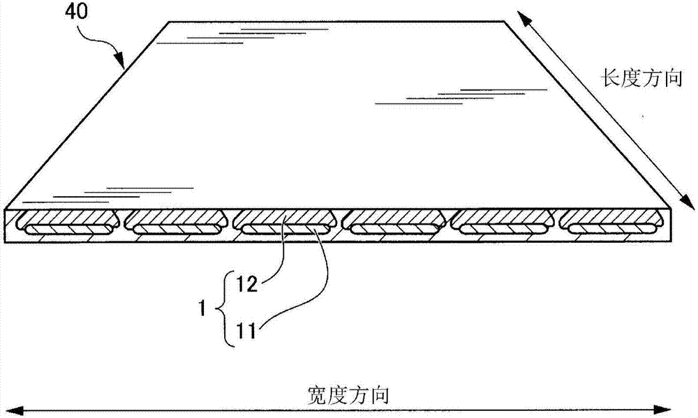
The film-forming substrates molded to a predetermined size are embedded side by side in the connection substrate, connected and integrated, and the intermediate layer, superconducting layer, and protective layer are laminated on the film-forming surface side of the film-forming substrate, and then the following steps are performed: method, etc. to manufacture superconducting conductors, that is: winding one or more integrated superconducting conductors on a prescribed core material; Winding one or more wires on the core material; and alternately winding integrated and non-integrated wires, etc., obtains a superconducting conductor having good superconducting properties without shape problems such as local protrusions.

Description

technical field [0001] The invention relates to a superconducting wire conductor used for superconducting equipment such as a superconducting cable or a superconducting magnet and a manufacturing method of the superconducting conductor. Background technique [0002] In the past, many attempts have been made to form superconducting layers on substrates to produce superconducting wires. In addition, in order to obtain a superconducting wire having a desired wire width, there is a method of cutting a metal plate by slitting or the like, preparing a metal substrate of a desired width, forming an intermediate layer on the surface of the metal substrate, and A superconducting layer with good crystal orientation is formed on the surface of the intermediate layer. On the other hand, a superconducting wire obtained by forming an intermediate layer and a superconducting layer on a metal substrate wider than a desired width may be further thinned. In this case, a laser cutting method...

Claims


Application Information

Patent Timeline
Patent Type & Authority Patents(China)
IPC IPC(8): H01B13/00H01B12/06H01F6/06
CPCH01F6/06H01B1/026H10N60/203H10N60/0464H10N60/0576H10N60/0801Y02E40/60H10N60/0632H01B12/02H05K3/10H05K3/26
Inventor 长洲义则
Owner FURUKAWA ELECTRIC CO LTD
Learn More