Cu/graphene delamination method based on femtosecond laser technology
A femtosecond laser and graphene technology, applied in the field of graphene preparation, can solve the problems of low yield and low efficiency, and achieve the effect of improved quality, uniform temperature and improved quality
- Summary
- Abstract
- Description
- Claims
- Application Information
AI Technical Summary
Problems solved by technology
Method used
Image
Examples
Embodiment 1
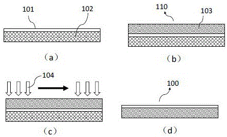
[0035] figure 1 It is a process flow chart of Cu / graphene exfoliation method based on femtosecond laser technology. Use CVD technology to deposit a layer of graphene 101 on the surface-treated 200um thick copper foil 102, such as figure 1 As shown in (a); the target substrate (PMMA material) 103 is bonded to graphene 101 to obtain a three-layer structure 110 of Cu / graphene / target substrate, as figure 1 As shown in (b); adjust the spot size of the femtosecond laser beam 103, and pass through the transparent target substrate (the purpose of using the femtosecond laser is to focus the laser on the interface layer, copper is opaque, so the laser cannot enter, so It must be irradiated from a transparent material) Focus on the interface between the graphene 101 and the copper foil 102, scan from the edge of the three-layer structure 110 for laser irradiation until it is completed, and the copper foil can be removed, such as figure 1 as shown in (c); as figure 1 (d) shows the exfo...
Embodiment 2
[0038] Use PECVD technology to deposit a layer of graphene 101 on the 10um thick copper foil 102 through surface treatment; The target substrate (its material is SiO 2 ) 103 and graphene 101 are directly bonded to obtain a three-layer structure 110 of Cu / graphene / target substrate; adjust the spot size of the femtosecond laser beam 103, and pass through the transparent target substrate (the purpose of using femtosecond laser It is to focus the laser on the interface layer, copper is opaque, so the laser cannot enter, so it must be irradiated from a transparent material) Focus on the interface between graphene 101 and copper foil 102, from the edge of the three-layer structure 110 Start scanning for laser irradiation until complete, the copper foil can be removed, and the exfoliated graphene and target substrate can be obtained.
Embodiment 3
[0040] The difference from Embodiment 1 is that the thickness of the copper foil is 100 um, and the material of the transparent target substrate is SiN.
PUM
| Property | Measurement | Unit |
|---|---|---|
| thickness | aaaaa | aaaaa |
| breaking strength | aaaaa | aaaaa |
| electrical resistivity | aaaaa | aaaaa |
Abstract
Description
Claims
Application Information
