Colored filter layer, display substrate and display device

A color filter layer and display substrate technology, which is applied in optics, nonlinear optics, instruments, etc., can solve the problems of low light source utilization rate and narrow display color gamut, and achieve the effect of improving utilization rate and avoiding waste

Active Publication Date: 2015-11-11
BOE TECH GRP CO LTD
View PDF5 Cites 56 Cited by
  • Summary
  • Abstract
  • Description
  • Claims
  • Application Information

AI Technical Summary

Problems solved by technology

[0004] The inventors have found that there are at least the following problems in the prior art: the existing display products usually use a white light-emitting diode backlight and an ordinary color filter layer to form a color display, but the utilization rate of the light source in this color display method is low, and Displays with a narrow color gamut

Method used


Image

  • Colored filter layer, display substrate and display device
  • Colored filter layer, display substrate and display device
  • Colored filter layer, display substrate and display device

Examples


Embodiment 1

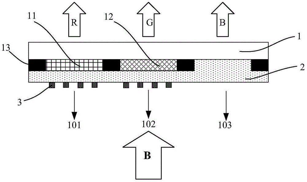
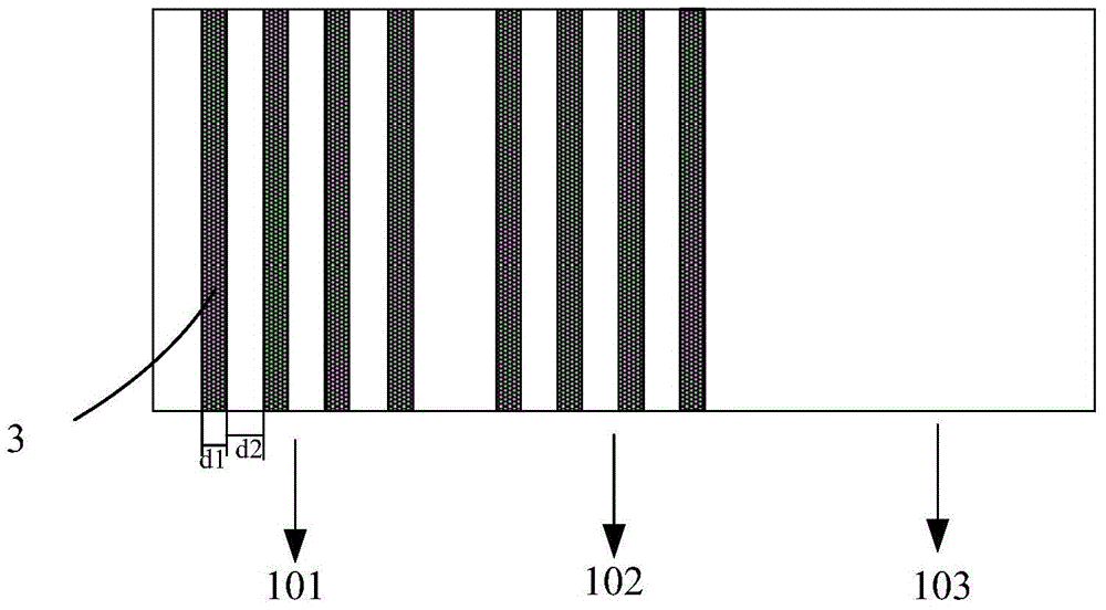
[0042] like figure 1 and 2 As shown, this embodiment provides a color filter layer, which includes a substrate 1, a color filter disposed on the substrate 1, a planarization layer 2 disposed above the layer where the color filter is located, and a planarization layer 2 disposed on the planarization layer. The filter layer 3 above the layer 2; wherein, the color filter of this embodiment includes a red light unit 101, a green light unit 102, and a blue light unit 103, and the three are arranged alternately; the red light unit 101 includes: red quantum dots Layer 11; the red quantum dot layer 11 is used to emit red light R under the excitation of blue light B; the green light unit 102 includes: a green quantum dot layer 12; the green quantum dot layer 12 is used to emit under the excitation of blue light B Green light G; the blue light unit 103 is not covered with a quantum dot layer, and is used to transmit blue light B; the filter layer 3 in this embodiment is at least locate...

Embodiment 2

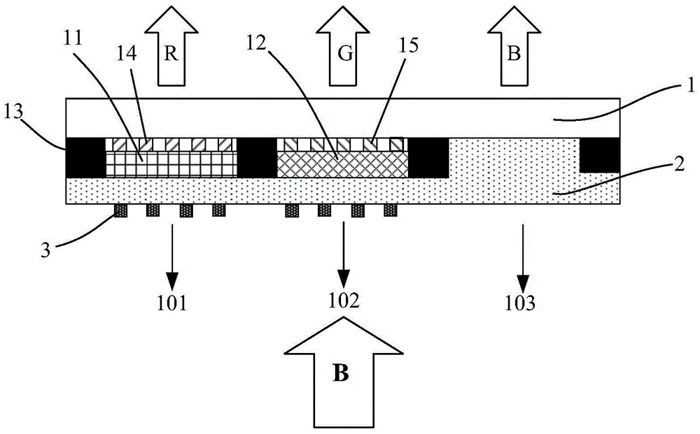
[0051] like image 3 and 4 As shown, this embodiment provides a color filter layer, the structure of which is roughly the same as that of the color filter layer in Embodiment 1, the difference lies in the structure of the red light unit 101 and the green light unit 102 .

[0052] Specifically, the red light unit 101 in this embodiment includes a first blue light filter layer 14 and a red quantum dot layer 11 sequentially arranged on the substrate 1; the green light unit 102 includes a second blue light filter layer sequentially arranged on the substrate 1 15 and green quantum dot layer 12. Wherein, the first blue light filter layer 14 is used to filter out the blue light B passing through the red quantum dot layer 11 ; the second blue light filter layer 15 is used to filter out the blue light B passing through the green quantum dot layer 12 .

[0053] The reason why the first blue light filter layer 14 is set between the substrate 1 and the red quantum dots is that when the...

Embodiment 3

[0061] This embodiment provides a display substrate and a display device; wherein the display substrate includes the color filter layer described in Embodiment 1 or 2; the display substrate can be a color filter substrate or a COA (colorfilteronarray) substrate.

[0062] The display device provided in this embodiment includes the above-mentioned display substrate, so the display effect of the display device in this embodiment is better.

[0063] The display device can be any product or component with a display function such as a liquid crystal panel, an electronic paper, an OLED panel, a mobile phone, a tablet computer, a television, a monitor, a notebook computer, a digital photo frame, a navigator, and the like.


PUM

PropertyMeasurementUnit
thicknessaaaaaaaaaa
thicknessaaaaaaaaaa
particle diameteraaaaaaaaaa

Abstract

The invention provides a colored filter layer, a display substrate and a display device and belongs to the technical field of displaying. The colored filter layer, the display substrate and the display device can solve the problem that the utilization rate of a light source of an existing display device is low. The colored filter layer comprises a base and a colored filter arranged on the base. The colored filter includes a red unit, a green unit and a blue unit, wherein the red unit comprises a red quantum dot layer used for giving off red light under the stimulation of blue light, the green unit comprises a green quantum dot layer used for giving off green light under the stimulation of blue light, and the blue unit is not covered with a quantum dot layer and used for enabling blue light to be transmitted. The colored filter layer further comprises a planarization layer arranged on the colored filter and a smoothing layer which is located on the planarization layer and at least located at the position corresponding to the red unit and the green unit. The smoothing layer is used for filtering light except blue light out.

Description

technical field [0001] The invention belongs to the field of display technology, and in particular relates to a color filter layer, a display substrate and a display device. Background technique [0002] Quantum Dot (QuantumDot) is a semiconductor nanostructure that binds conduction band electrons, valence band holes, and excitons in three spatial directions. This constraint can be attributed to electrostatic potential (by external electrodes, doping, strain , impurity generation), the interface of two different semiconductor materials (for example: in self-assembled quantum dots), the surface of a semiconductor (for example: semiconductor nanocrystals), or a combination of the above three. Quantum dots have separate quantized energy spectra, corresponding to wave functions that are spatially located in the quantum dot, but extend over several lattice periods. A quantum dot has an integer number (1-100) of electrons, holes or hole-electron pairs, that is, the electric charg...

Claims


Application Information

Patent Timeline
Patent Type & Authority Applications(China)
IPC IPC(8): G02F1/1335G02F1/13357
CPCG02F1/133509G02F1/133617
Inventor 谷新姚继开金起满
Owner BOE TECH GRP CO LTD
Why Eureka
Try Eureka