Array substrate, production method thereof, display panel and display device

A technology of an array substrate and a manufacturing method, applied in the display field, can solve problems such as the adverse effect of packaging, and achieve the effects of improving yield, reducing the probability of breakage, and improving adhesion strength

Active Publication Date: 2015-11-18
BOE TECH GRP CO LTD
View PDF6 Cites 6 Cited by
  • Summary
  • Abstract
  • Description
  • Claims
  • Application Information

AI Technical Summary

Problems solved by technology

[0003] The current OLED display panel mainly includes a packaging substrate and an array substrate. OLED devices are formed on the array substrate. A sealing structure is formed between the packaging substrate and the array substrate through packaging technology. The current packaging technology mainly includes glass frit packaging technology and RTB (Room Temperature Bonding , room temperature bonding) technology, see figure 1 , figure 1 It is an OLED display panel formed by RTB packaging technology. It forms a room temperature bonding layer 210' on the packaging area of ​​the packaging substrate 200', forms a room temperature bonding layer 120' on the packaging area of ​​the array substrate 100', and then aligns the two Pressing to form a sealing structure between the two substrates, wherein, since the surface of the packaging area of ​​the array substrate is usually formed with uneven peripheral circuits, in order to improve the packaging yield, it is necessary to form a sealing structure on the packaging area of ​​the array substrate before packaging. However, during encapsulation, if there is dust or other defects on the surface of the formed encapsulation planar layer, it will also adversely affect the effect of encapsulation.

Method used


Image

  • Array substrate, production method thereof, display panel and display device
  • Array substrate, production method thereof, display panel and display device
  • Array substrate, production method thereof, display panel and display device

Examples


Embodiment Construction

[0028] The specific implementation manners of the present invention will be further described in detail below in conjunction with the accompanying drawings and embodiments. The following examples are used to illustrate the present invention, but are not intended to limit the scope of the present invention.

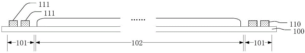
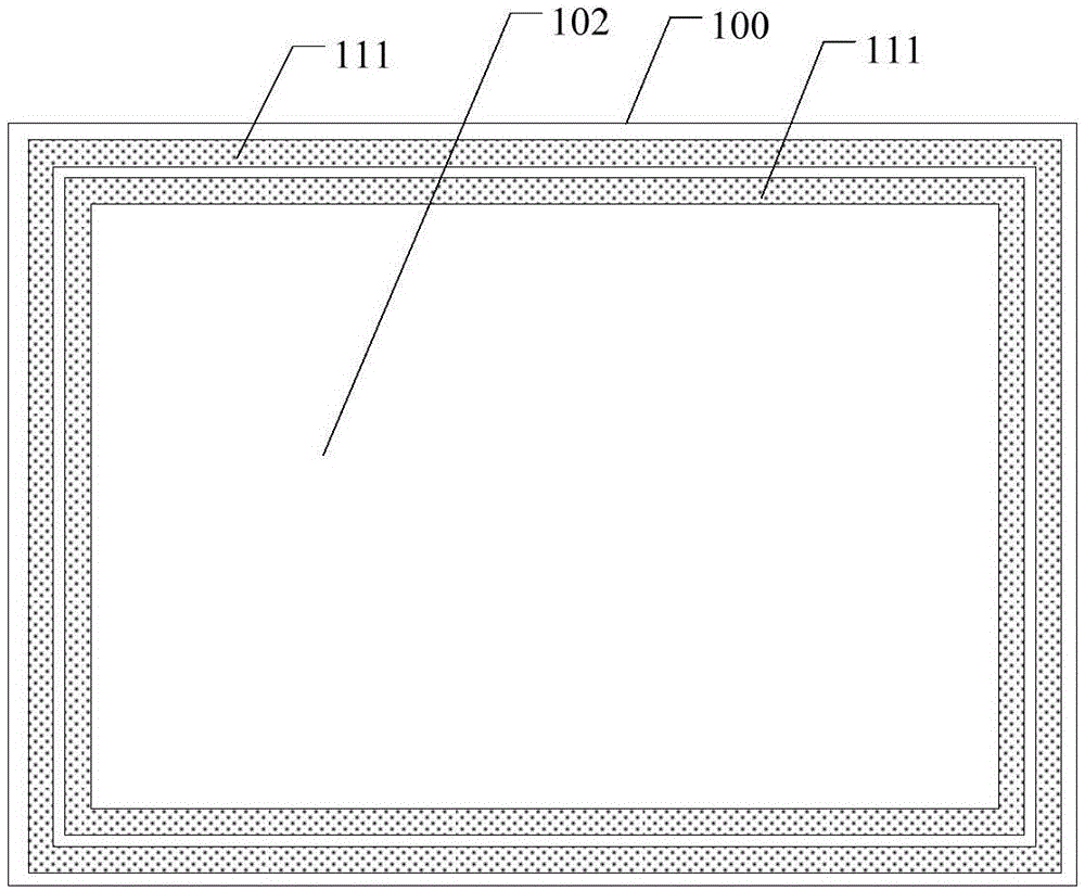
[0029] An embodiment of the present invention provides an array substrate, the array substrate includes a display area and a packaging area surrounding the display area, the packaging area is provided with a packaging flat layer, and the packaging flat layer includes a plurality of packaging flat units, Each encapsulation flat unit forms a ring pattern on the encapsulation area and surrounds the display area.

[0030] In the array substrate provided by the embodiment of the present invention, by setting the packaging flat layer in the packaging area as a plurality of annular packaging flat units, in the subsequent packaging process, not only can the contact area between th...


PUM


Abstract

The invention provides an array substrate, a production method thereof, a display panel and a display device. The array substrate includes a display area and a packaging area surrounding the display area; the packaging area is provided with a packaging flat layer; the packaging flat layer comprises a plurality of packaging flat units; and each packaging flat unit forms an annular pattern on the packaging area and surrounds the display area. With the array substrate of the invention adopted, the contact area of a formed normal-temperature bonding layer and the packaging flat layer can be increased, and the strength of a bonding force between the normal-temperature bonding layer and the packaging flat layer can be improved; the packaging flat layer is divided into a plurality of unit structures which are independent from each other, even if dust or other defects exist on the surface of one unit structure, the sealing performance of the other unit structures and the normal-temperature bonding layer has little possibility of being adversely affected, and therefore, the yield of a packaging process can be improved.

Description

technical field [0001] The present invention relates to the display field, in particular to an array substrate and a manufacturing method thereof, a display panel, and a display device. Background technique [0002] Organic Light Emitting Diode (OLED) display panel has many advantages such as active light emission, high brightness, high contrast ratio, ultra-thin, low power consumption, large viewing angle and wide operating temperature range. It is an advanced new flat panel display with wide application. device. [0003] The current OLED display panel mainly includes a packaging substrate and an array substrate. OLED devices are formed on the array substrate. A sealing structure is formed between the packaging substrate and the array substrate through packaging technology. The current packaging technology mainly includes glass frit packaging technology and RTB (Room Temperature Bonding , room temperature bonding) technology, see figure 1 , figure 1 It is an OLED display...

Claims


Application Information

Patent Timeline
Patent Type & Authority Applications(China)
IPC IPC(8): H01L27/32H01L21/77G09G3/30
CPCH10K59/12H10K50/8426H10K59/1201
Inventor 藤野诚治张嵩高静王涛杜小波
Owner BOE TECH GRP CO LTD
Why Eureka
Try Eureka