Mask plate, fabrication method thereof and exposure system

A mask plate and mask technology, which is applied in photolithography exposure devices, microlithography exposure equipment, optics, etc., can solve the problems of source-drain channel disconnection, thin resist, and thin-film transistor inoperability, etc. Achieve the effect of improving exposure quality and improving quality

Pending Publication Date: 2015-11-25
BOE TECH GRP CO LTD +1
View PDF6 Cites 14 Cited by
  • Summary
  • Abstract
  • Description
  • Claims
  • Application Information

AI Technical Summary

Problems solved by technology

[0004] On the TFT-LCD array substrate, such as figure 1 As shown, since the distribution density of thin film transistors in the non-display area 5 (such as the peripheral wiring area) is much higher than that of the display area 6 (ie, the pixel area), so in the process of developing after exposure, the non-display area 5 has a negative impact on the development per unit time. The consumption of the liquid is much lower than that in the display area 6, which makes the concentration of the developer in the local area in the non-display area 5 higher than that in the display area 6, so that the photolithography of the channel area of ​​the thin film transistor in the non-display area 5 is easily caused after the development is completed. The glue is too thin, and after the etching process, it is easy to cause the source-drain channel semiconductor to be missing, so that the source-drain channel is disconnected, so that the thin-film transistors in the non-display area 5 of the TFT-LCD cannot work, and eventually the display area 6 cannot be used. normal display

Method used


Image

  • Mask plate, fabrication method thereof and exposure system
  • Mask plate, fabrication method thereof and exposure system

Examples


Embodiment 1

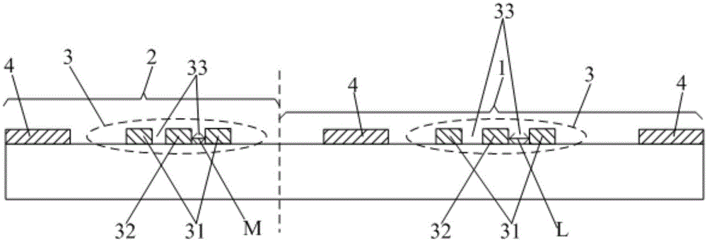
[0037] This embodiment provides a mask, such as figure 2 As shown, it includes a transparent substrate (not marked) and a mask pattern formed on the surface of the transparent substrate.

[0038] Wherein, the mask pattern includes a first area 1 for correspondingly forming the film layer pattern in the display area and a second area 2 for correspondingly forming the film layer pattern in the non-display area;

[0039] Both the first area 1 and the second area 2 are provided with a plurality of patterned masks 3, and the distribution density of the patterned masks 3 in the first area 1 is smaller than the distribution density of the patterned masks 3 in the second area 2;

[0040] Each patterned mask 3 includes a first pattern 31 for forming the source of the transistor, a second pattern 32 for forming the drain of the transistor, and a pattern interposed between the first pattern 31 and the second pattern 32. The slit 33; the width L of the slit 33 in the first zone 1 is gre...

Embodiment 2

[0060] This embodiment provides an exposure system, including the mask plate in Embodiment 1.

[0061] By using the mask plate in embodiment 1, the exposure quality of the exposure system is improved, thereby improving the quality of products exposed by the exposure system.


PUM


Abstract

The invention provides a mask plate, a fabrication method thereof and an exposure system. The mask plate comprises a first region and a second region, wherein a plurality of patterning masks are arranged in both of the first region and the second region, and the distribution density of the plurality of patterning masks in the first region is smaller than the distribution density of the plurality of patterning masks in the second region; and each patterning mask comprises a first pattern, a second pattern and a slit between the two patterns, and the slit width in the first region is greater than the slit width in the second region. By the mask plate, the intensity of the exposure light ray penetrating through the slit in the second region is reduced relative to the intensity of the exposure light ray penetrating through the slit in the first region, thus, the thickness of a photoresist reserved on an active region film layer tends to consistency after transistors in a display region and a non-display region are exposed and developed through a source and a drain, an active region of the transistor in the non-display region after being subjected to an etching process is further ensured not to be broken, and finally, the transistor in the non-display region can be ensured to normally work.

Description

technical field [0001] The present invention relates to the field of display technology, in particular to a mask plate, a preparation method thereof, and an exposure system. Background technique [0002] In a thin film transistor liquid crystal display (TFT-LCD), the thin film transistor plays a very important role as a switching device of a digital circuit. [0003] At present, in the production of TFT-LCD array substrates, a single-slit diffraction mask (SingleSlitMask), a gray-tone mask (GrayToneMask) or a half-tone mask (HalfToneMask) is generally used for the source-drain metal layer mask (SDMask) process. When a single-slit diffraction mask is used for the source-drain metal layer masking process, the source-drain channel region is exposed through slit diffraction. Since the source-drain channel itself is relatively narrow, if the light intensity of the exposure light is too low after diffracting through the slit and the exposure is insufficient, it is easy to cause t...

Claims


Application Information

Patent Timeline
Patent Type & Authority Applications(China)
IPC IPC(8): G03F1/32G03F7/20
CPCG03F1/32H01L27/124H01L27/1288H01L27/1262H01L27/1214H01L27/127H01L29/458H01L29/4908
Inventor 罗丽平刘会双胡海琛孙增标王涛金基用
Owner BOE TECH GRP CO LTD
Why Eureka
Try Eureka