

Etching method
A technology for etching gas and grooves, which is applied in the direction of electrical components, semiconductor/solid-state device manufacturing, circuits, etc., can solve the problems of limited passivation effect, short gas introduction time, etc., to reduce the lateral etching speed and reduce side effects. Wall bending phenomenon, the effect of improving product quality
- Summary
- Abstract
- Description
- Claims
- Application Information
AI Technical Summary
Problems solved by technology
Method used
Image

Examples
specific Embodiment approach
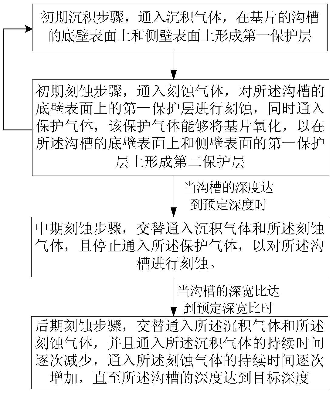
[0040] As a specific embodiment of the present invention, the temperature in the etching method is 20°C±1°C, and the process parameters in the initial deposition step are: the pressure in the process chamber is 15mT-70mT; 1000W-2000W to ionize the deposition gas into plasma; the flow rate of the deposition gas is 120sccm-200sccm; the deposition time is 2s-6s.
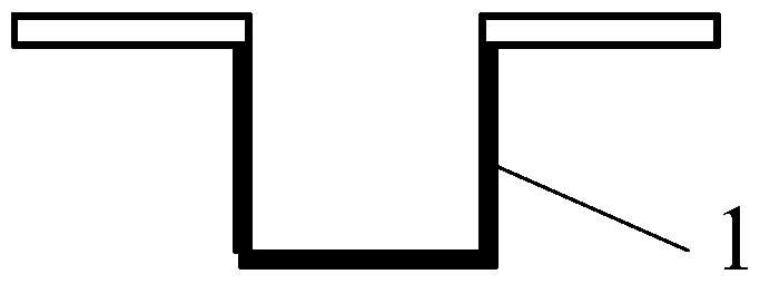
[0041] In the present invention, the initial etching step may include etching the first protective layer 1 on the bottom wall surface of the trench, and when the first protective layer 1 is etched away, continue to etch the first protective layer 1 underlying substrate material. That is, the initial etching step may include:
[0042] S101. Adjust the power of the upper radio frequency power supply and the lower radio frequency power supply, and inject the etching gas to etch away the first protective layer 1 formed on the bottom wall surface of the trench, exposing the material of the substrate;
[0043]S102. Adjust t...
PUM
 Abstract
Description
Claims
Application Information