N-channel non-volatile flash memory device and compiling, erasing and reading method thereof

A non-volatile, flash memory device technology, used in electrical solid-state devices, semiconductor devices, semiconductor/solid-state device manufacturing, etc. Small, reduce electron surplus, solve the effect of erasing saturation problem

Active Publication Date: 2015-11-25
SHANGHAI HUALI MICROELECTRONICS CORP
View PDF4 Cites 5 Cited by
  • Summary
  • Abstract
  • Description
  • Claims
  • Application Information

AI Technical Summary

Problems solved by technology

[0006] The object of the present invention is to overcome the above-mentioned defect that prior art exists, provide a kind of N-channel non-volatile flash memory device and compiling, erasing and reading method thereof, can overcome the erasing problem that existing p-channel B4-Flash exists Eliminate the problem of saturation, and solve the problem of high power consumption in the existing channel hot electron injection programming by using low-power programming and erasing methods

Method used


Image

  • N-channel non-volatile flash memory device and compiling, erasing and reading method thereof
  • N-channel non-volatile flash memory device and compiling, erasing and reading method thereof
  • N-channel non-volatile flash memory device and compiling, erasing and reading method thereof

Examples


Embodiment Construction

[0033] The specific embodiment of the present invention will be further described in detail below in conjunction with the accompanying drawings.

[0034] It should be noted that, in the following specific embodiments, when describing the embodiments of the present invention in detail, in order to clearly show the structure of the present invention for the convenience of description, the structures in the drawings are not drawn according to the general scale, and are drawn Partial magnification, deformation and simplification are included, therefore, it should be avoided to be interpreted as a limitation of the present invention.

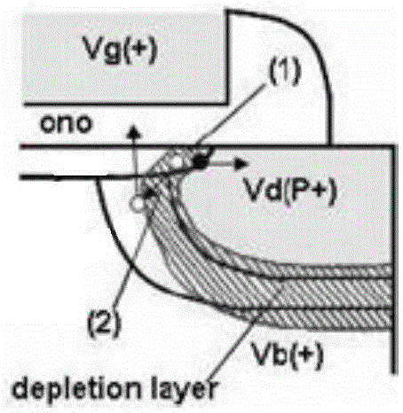
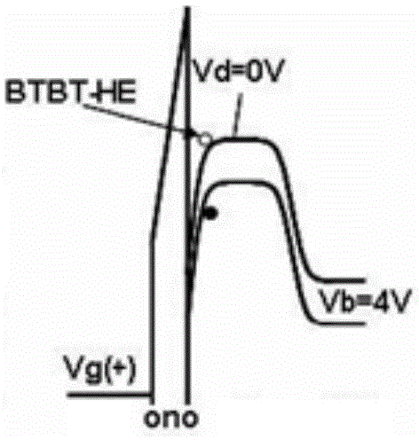
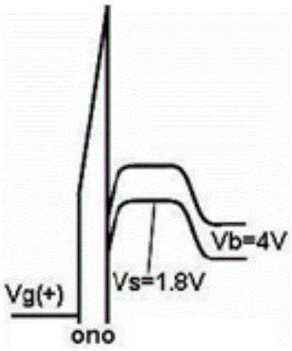
[0035] In the following specific embodiments of the present invention, please refer to figure 2 , figure 2 It is a structural schematic diagram of an N-channel non-volatile flash memory device in a preferred embodiment of the present invention. Such as figure 2As shown, an N-channel non-volatile flash memory device of the present invention incl...


PUM


Abstract

The invention discloses an N-channel non-volatile flash memory device and a compiling, erasing and reading method thereof. The N-channel non-volatile flash memory device includes a P type silicon substrate with an N type doped source end, a drain end and an N channel which are formed therein, and a gate structure which is formed on the substrate and is located between the source end and the drain end and includes a gate oxide layer, a polysilicon floating gate, a first silicon oxide layer, a silicon nitride layer, a second silicon oxide layer and a polysilicon control gate which are distributed sequentially from bottom to top, wherein the polysilicon floating gate is used for storing charges. According to the flash memory device provided by the invention, a low-power consumption band-to-band-tunneling hot-hole injection compiling and channel FN electron tunneling erasing method is adopted, and therefore, the problem of high consumption of original channel hot electron injection programming can be solved, and a traditional floating gate transistor structure can have a smaller gate length, and the problem of erasure saturation which cannot be solved by a traditional p-channel B4-Flash can be solved, and the N-channel non-volatile flash memory device can be manufactured more easily.

Description

technical field [0001] The present invention relates to the technical field of semiconductor memory, more specifically, to a non-volatile flash memory device with an N-type doped channel and its compiling, erasing and reading methods. Background technique [0002] For the NOR flash memory unit, the most important factor limiting the further reduction of its size is the further shortening of the gate length. This is mainly because the compilation method of channel hot electron (CHE) injection used in NOR flash memory cells requires a certain voltage at the drain of the device, and this voltage has a great impact on the penetration of the source and drain. Therefore, channel hot electron (CHE) injection is not suitable for short-channel devices. Another problem is that NOR flash memory is limited by the programming rate compared with NAND and AND data storage devices. According to the prediction of the document "G. Servalli, et al., IEDMTech. Dig., 35_1, 2005", the physical ...

Claims


Application Information

Patent Timeline
Patent Type & Authority Applications(China)
IPC IPC(8): H01L27/115H01L21/8247
Inventor 顾经纶彭兴伟
Owner SHANGHAI HUALI MICROELECTRONICS CORP
Why Eureka
Try Eureka