A photoelectric conversion circuit applied to mouse equipment

A technology of photoelectric conversion circuits and equipment, applied in the direction of analog-to-digital converters, etc., can solve the problems of weak output electrical signal strength, large occupied area, and high cost, and achieve the effects of enhancing photoelectric performance, reducing occupied area, and reducing costs

Active Publication Date: 2018-11-27
CRM ICBG (WUXI) CO LTD
2 Cites 0 Cited by

AI-Extracted Technical Summary

Problems solved by technology

However, simply using CMOS image sensing technology for photoelectric conversion does not take into account the linear conversion problem between photoelectric signals, resulting in the inability to effectively convert optical signals into electrical signals in the nonlinear region; an...

Method used

The present invention has increased the constant current source circuit in Fig. 2, can adapt to the amplitude of different sampling voltages, promptly adapts to different current characteristics; After resistance dividing in Fig. 5, the off-line voltage VL1 input of ADC module To the VRL of AMP2 in Figure 4, by changing the ratio ...

Abstract

The invention relates to a field of photoelectric technologies, and specifically relates to a photoelectric conversion circuit applied to mouse equipment. The photoelectric conversion circuit comprises a PD pipe array module, a buffer amplifier module and an ADC (Analog to Digital Converter) module; the photoelectric conversion circuit is characterized in that a row-column gating signal of the PD pipe array module is provided by a peripheral time sequence generation circuit; an output end of the PD pipe array module is connected with an input end of the buffer amplifier module; an output end of the buffer amplifier module is connected with an input end of the ADC module; the output end of the buffer amplifier module is connected with a peripheral DSP (Digital Signal Processor); the peripheral DSP controls the time sequence generation circuit to work. The photoelectric conversion circuit applied to the mouse equipment provided by the invention can be applied to different photoelectric current characteristics and enhances the photoelectric performance of an optical mouse; meanwhile, the varying optical signals can be totally converted into digital signals without omission; besides, two stage conversion is adopted to an ADC circuit, thus the area can be effectively reduced.

Application Domain

Technology Topic

Image

  • A photoelectric conversion circuit applied to mouse equipment
  • A photoelectric conversion circuit applied to mouse equipment
  • A photoelectric conversion circuit applied to mouse equipment

Examples

  • Experimental program(1)

Example Embodiment

[0015] The specific implementation and working principle of the present invention will be further described below in conjunction with the drawings and preferred solutions.
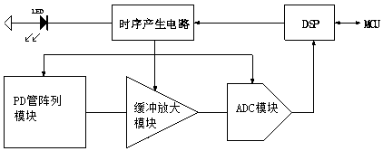
[0016] Such as figure 1 Shown is a schematic block diagram of the circuit connection peripheral structure of the present invention. This figure shows the principle diagram of applying the conversion circuit of the present invention to a specific circuit. The working principle of the figure is: the photodiode array module converts the optical signal into an electrical signal. After being amplified by the buffer and amplifying module, the electrical signal is converted into a digital signal by the ADC conversion module and input to the peripheral structure DSP. DSP and MCU are serialized Bus interface, receiving MCU setting instructions and sending displacement information data to MCU. At the same time, DSP also controls the work of the timing generating circuit, receiving and processing the data converted by the ADC conversion module. The timing generating circuit is mainly composed of flip-flops to generate regular photoelectric The row and column strobe signal of the diode array reads the status of the 24*24 photodiodes one by one.
[0017] Such as figure 2 Shown is an implementation figure 1 The internal principle diagram of the photodiode array module in the middle, that is, the readout principle diagram of the photodiode array row and column strobe signals. The photodiode array module specifically includes diodes, capacitors, and ten NMOS transistors. The tubes are: N0 tube, N1 tube, N2 tube, N3 tube, N4 tube, N5 tube, N6 tube, N7 tube, N8 tube, N9 tube. In the figure, the current IB1 and IB2 are provided by the BIAS_AMP buffer amplifier module, through the N7 tube, The N8 tube and N9 tube constitute a current mirror circuit. The drain of the N7 tube is connected to the gate and is also connected to the gate of the N8 tube. The drain of the N7 tube is also used as the input of the bias current IB1. The N8 tube and the N9 tube In series connection, the gate of the N9 tube is connected to the drain of the N8 tube, and the bias voltage VBL is output. The drain of the N8 tube is also used as the input of the bias current IB2. The source of the N7 tube and the source of the N9 tube are both grounded. The mirror circuit provides a constant current for the photodiode array module. By changing the size of the current, the charge and discharge speed of the W3 potential can be adjusted. The photoelectric signal sampling and amplification is divided into two cyclic processes: sampling after exposure and amplification after reset. The N0 tube, N1 tube, N2 tube, N5 tube, and N6 tube form a photoelectric linear conversion circuit. The N3 tube and N4 tube form a constant current source circuit. The drain of the N0 tube is connected to the power supply, and the gate is connected to the reset signal. RST, the source is connected to the negative terminal of the diode, while the source of the N0 tube is connected to the gate of the N1 tube, the drain of the N1 tube is connected to the power supply, the source of the N1 tube is connected to the drain of the N2 tube, and the gate of the N2 tube is connected to the selection Pass the signal SEL, the source of the N2 tube is connected to the drain of the N3 tube, and at the same time to the positive plate of the capacitor, the gate of the N3 tube is connected to the bias voltage VBH, the N3 tube is connected in series with the N4 tube, and the source of the N4 tube is grounded, and N4 The gate of the tube is connected to the bias voltage VBL, the drain of the N5 tube and the N6 tube are connected to the negative plate of the capacitor, the gate of the N5 tube is connected to the strobe signal SEL1, the source outputs the reference voltage VREF, and the gate of the N6 tube is connected to the selective communication No. SEL2, the source outputs the output voltage PD_VOUT of the photodiode array module. In the constant current source circuit composed of N3 tube and N4 tube, the reset signal RST is high first, and the potential of the cathode voltage W1 of the photodiode is charged to a threshold voltage of the NMOS tube lower than VDDA. Set the turn-on voltage to Vthn, then The voltage at point W1 is approximately: V(W1)=V(VDDA)-Vthn; then the reset signal RST changes from high to low, and DSP controls the external LED to light up for a period of time (about 8μs~190μs, automatically by DSP Adjust) to perform exposure sampling. During this period, the DIODE diode in the photodiode array module is discharged by the external LED light. The degree of discharge is related to the light time and intensity. At this time, the strobe signal SEL, SEL1 is pulled to high potential, N2 tube, N5 tube is strobed, N1 tube acts as a voltage follower, the potential of C2 right plate W4 is pulled to VREF, and the potential of W1 follows the photodiode The discharge potential drops. Assuming that the potential of W1 drops by ΔV1 during the discharge period, the voltage value of the left plate W3 of C2 at this time is: V(W3)=V(VDDA)-2×Vthn-ΔV, at this time the voltage of the left plate of C2 Is V(W3), the voltage of the right plate is VREF, then SEL1 is pulled to a low level, SEL2 is pulled to a high level, at the same time the RST signal goes to a high level, and the W1 potential is pulled up, rising by ΔV1, W2, The potential of W3 is also pulled up by ΔV along with the potential of W1. After reset, the voltage of W3 is: V(W3)=V(VDDA)-2×Vthn, then the potential of C2 right plate W4 also rises from VREF ΔV, VOUT increases with the potential of W4 by ΔV at the same time.
[0018] From the above analysis, it can be seen that the N3 tube and N4 tube need to work in the saturation region to provide a constant current I for the circuit. By changing the size of the current, the charge and discharge speed of the capacitor can be changed to adapt to the amplitude of different sampling voltages, N1 tube, N2 tube The tube needs to work in the linear amplification zone to maintain a linear relationship between ΔV and ΔV1, and VOUT linearly reflects the change of W1 potential.
[0019] correspond figure 2 The working sequence diagram in, such as image 3 As shown, RST is high at T1, and W1 is pulled to high; when LED is low at T2, the photodiode receives light to discharge, W2 is kept at a low potential after discharge, and the T2 time is adjusted by DSP; after the discharge is over At T3, SEL is at a high potential, and the low potential of W2 is transferred to W3. The potential of W3 is the low potential after discharge. At the same time, SEL1 is pulled high, and the potential of W4 is pulled to VREF; then at T4, RST is again high and W1 is Pulled high, W3 potential follows W1 to be pulled high, while SEL1 is low, and W4 is released, the potential will follow W3, SEL2 is high, and VOUT follows W4. Since the voltage of each pixel is converted by ADC in turn, the minimum T4 time is 1.7us , The maximum is 6uS, so far one cycle ends.
[0020] Such as Figure 4 Shown is an implementation figure 1 The schematic diagram of the middle buffer amplifier module. The output currents I11 and I12 in the bias current generating circuit provide bias currents for the differential input amplifier and common source amplifier of AMP1, and I21 and I22 provide bias for the differential input amplifier and common source amplifier of AMP2. Current, IB1, IB2, IB3 provide bias current for the outside world. The operational amplifier AMP2 is a voltage follower, the VRL input terminal is input to the forward input terminal of the operational amplifier AMP2 through the resistor R0, and the voltage follower output terminal is connected to the B terminal of a series of resistors, so that the voltage at point B follows VRL. The operational amplifier AMP1 is used as a proportional operation amplifier with the same direction. Its positive input terminal is connected to the photodiode _VOUT, and the reverse input terminal is indirectly connected to the C terminal of the column resistor through a 3-wire-8-wire decoder, and is input through the decoder End MAG_FCT <2:0> The choice of can adjust the position of C terminal, thereby changing the resistance ratio between AC and BC, thereby adjusting the output voltage of AMP_OUT terminal, Known from the photodiode array module: V PD _OUT=V REF +ΔV, in the ADC module, VREF is obtained by dividing the voltage of the VRL resistor: V REF =K×V VRL (K≤1), K=1 in the ideal state, ΔV is the voltage difference during the photodiode exposure reset process, which can be obtained by the above formula: It can be seen from the above formula that the BIAS_AMP buffer amplifier module takes VRL as the lowest voltage to selectively amplify the voltage difference of the photodiode, and the amplification factor is A. VRL is output by the ADC module and is the lower limit voltage during AD conversion. When the voltage at the AMP_OUT terminal is less than the upper limit voltage of the ADC module, A×ΔV, that is, the linear change of the voltage during the photodiode exposure reset process, can be converted into a digital value. Adjust K to keep the output voltage of the AMP_OUT terminal within the upper and lower limit voltage range of the ADC.
[0021] Such as Figure 5 Shown is an implementation figure 1 The schematic diagram of the ADC module in the middle, the BIAS_AMP buffer amplifier module output port AMP_OUT output voltage analog quantity is converted into DAT <6:0> Digital quantity, this structure performs two-level conversion, the first level conversion gets the high four bits of the digital signal, and the second level conversion gets the low three bits of the digital signal. The operational amplifier OPAMP0 constitutes a voltage follower. The output voltage is equal to the positive input voltage VBG. The resistors R0~R17 divide VBG. VH1 and VL1 are the ADC input voltage ranges. The resistors R1~R16 have the same resistance value and limit the upper and lower power The voltage difference VH1-VL1 is divided into 16 equal parts, and each is compared with the voltage of the AMP_OUT port. If the voltage of the AMP_OUT port is greater than the divided voltage of the resistor, the comparator outputs a high potential, otherwise, it outputs a low potential. The photodiode _ARRAY and BIAS_AMP Module analysis shows that the output voltage of AMP_OUT port is between VH1 and VL1, assuming that the voltage of AMP_OUT port is at resistance R Between the voltages at both ends, the M-th comparator starts to output a high potential, that is, A1~A Output low potential, A ~A16 outputs high potential, the decoding circuit gets the high four-bit DAT of the output digital signal <6:3> , And R The voltages at both ends are output to VH2 and VL2 as the upper and lower limit voltages of the second stage conversion. Similarly, the voltage difference is divided into 7 equal parts through R21~R27, and each is compared with the AMP_OUT port voltage, and the number is obtained after decoding The third DAT of the signal <2:0> .
[0022] Such as Image 6 Shown is a bias current generating circuit of the present invention. AMP0, MP0 and R0 form a voltage follower circuit. The LDO module provides the input voltage VBG and bias current I0 for the op amp AMP0. When the VBG input voltage, both ends of R0 The voltage is equal to VBG, the appropriate current can be obtained by adjusting the resistance of R0, and the current source mirrored to the right provides bias currents IB1, IB2, IB3 to the outside world. The currents flowing through MP7 and MP8 are mirrored again by MN0 to generate currents Ibias1 and Ibias2, as shown in the figure below, when ENH1 is high, the ratio of the current flowing through MP9 is mirrored to MP11 and MP12, and the currents I11 and I12 are figure 2 The differential input amplifier and common source amplifier of AMP1 provide bias current, and the current flowing through MP15 is mirrored to MP21 and MP22. The currents I21 and I22 are figure 2 The differential input amplifier and common source amplifier of AMP2 provide bias current: I 21 = I bios2 , I 22 =3×I bios2 , The current flowing through MP9 is controlled by the I_CTRL signal. When I_CTRL is high, MP13 is cut off and IMP9 is equal to Ibias1. When I_CTRL is low, MP13 is on and Ibias1 is shunted. The aspect ratios of MP9 and MP10 are equal. At this time, The current IMP9 flowing through MP9 is half of Ibias1.
[0023] The invention adds figure 2 The constant current source circuit in, can adapt to different sampling voltage amplitudes, that is, adapt to different current characteristics; Figure 5 After the resistance is divided by the middle, the offline voltage VL1 of the ADC module is input to Figure 4 The VRL of AMP2 can amplify the electrical signal output by the photodiode array module and effectively limit it within the analog potential input range of the ADC module by changing the ratio of the resistance, that is, it can convert all the changed optical signals into digital signals without missing; The ADC module adopts two-level conversion, which effectively reduces the area.

PUM

no PUM

Description & Claims & Application Information

We can also present the details of the Description, Claims and Application information to help users get a comprehensive understanding of the technical details of the patent, such as background art, summary of invention, brief description of drawings, description of embodiments, and other original content. On the other hand, users can also determine the specific scope of protection of the technology through the list of claims; as well as understand the changes in the life cycle of the technology with the presentation of the patent timeline. Login to view more.

Similar technology patents

Preparation method of Ho-doped Bi2S3 nano-film

ActiveCN112939483AImprove photoelectric performanceRaw materials and equipment requirements are not highSemiconductor devicesThin membraneMethanol
Owner:GUILIN UNIVERSITY OF TECHNOLOGY

Classification and recommendation of technical efficacy words

  • Improve photoelectric performance
  • Small footprint
Why Eureka
Try Eureka