
Thin film transistor liquid crystal display

A liquid crystal display, thin film transistor technology, applied in instruments, nonlinear optics, optics, etc., can solve the problems of blistering on the upper polarizer, export of color filter substrates, poor conductivity between conductive silver glue and polarizer, etc. Effects of increased area, small ground impedance, reliable ESD path

Inactive Publication Date: 2015-12-02
AU OPTRONICS CORP
View PDF0 Cites 15 Cited by
  • Summary
  • Abstract
  • Description
  • Claims
  • Application Information

AI Technical Summary

Problems solved by technology

However, when the conductive silver adhesive is broken, this solution often causes poor contact between the polarizer and the ground wire of the array substrate, so that the static electricity on the color filter substrate cannot be discharged in time, and in severe cases, the arrangement of liquid crystal molecules will be affected. effect, resulting in pixel light leakage
In addition, if the contact area between the conductive silver glue and the polarizer is too small, it will easily lead to poor conductivity, or the coating position will cause bubbles on the edge of the upper polarizer, etc.

Method used


Image

  • Thin film transistor liquid crystal display
  • Thin film transistor liquid crystal display
  • Thin film transistor liquid crystal display

Examples


Embodiment Construction

[0027] In order to make the technical content disclosed in this application more detailed and complete, reference may be made to the drawings and the following various specific embodiments of the present invention, and the same symbols in the drawings represent the same or similar components. However, those skilled in the art should understand that the examples provided below are not intended to limit the scope of the present invention. In addition, the drawings are only for schematic illustration and are not drawn according to their original scale.

[0028] The specific implementation manners of various aspects of the present invention will be further described in detail below with reference to the accompanying drawings.

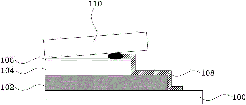
[0029] Figure 1A to Figure 1C The schematic diagrams respectively show the states of the connection modes of the three upper polarizers and the conductive silver glue in the thin film transistor liquid crystal display in the prior art. The following resp...


PUM


Abstract

The invention provides a thin film transistor liquid crystal display which comprises a first polarizer, an array substrate, a colored filter substrate, a second polarizer and conductive glue. The array substrate is located above the first polarizer, the colored filter substrate is opposite to the array substrate, a liquid crystal layer is clamped between the colored filter substrate and the array substrate, the second polarizer is located above the colored filter substrate, the side edge of the second polarizer is cut into a special shape, and the conductive glue is arranged between the second polarizer and the colored filter substrate in a coating mode. The side edge of the second polarizer, the side edge of the conductive glue and the side edge of the colored filter substrate further comprise silver glue which is electrically coupled with the second polarizer. Compared with the prior art, the side edge of the second polarizer is cut into the special shape such as a corrugated shape, so that the contact area of the conductive silver glue and the second polarizer is increased along with increasing of the length of a curve on the side edge of the second polarizer, smaller grounded impedance is obtained, and a more reliable electrostatic discharge path is formed.

Description

technical field [0001] The invention relates to a liquid crystal display technology, in particular to a thin film transistor liquid crystal display. Background technique [0002] The liquid crystal display device mainly includes a color filter substrate, an array substrate, a liquid crystal layer, a frame and a printed circuit board (PCB). Generally, a black matrix and a photoresist are arranged on the color filter substrate, thin film transistors (ThinFilmTransistor, TFT) are arranged on the array substrate, and spacers are arranged in the liquid crystal layer. During the manufacture and use of liquid crystal display devices, it is easy to generate static electricity and accumulate on the color filter substrate. When the static electricity accumulates to a certain extent, an electrostatic field will be generated. This electrostatic field will interfere with the electric field of the liquid crystal molecules inside the liquid crystal panel. The display screen is abnormal. ...

Claims


Application Information

Patent Timeline
Patent Type & Authority Applications(China)
IPC IPC(8): G02F1/1335
CPCG02F1/133514G02F1/133528G02F1/133531
Inventor 陈志明
Owner AU OPTRONICS CORP
Learn More