Arrayed waveguide grating spectrum planarization method
An arrayed waveguide grating and flattening technology, which is applied to optical waveguides, light guides, optics, etc., can solve the problems of narrow 3dB bandwidth and inability to make simple multi-channel large-scale arrayed waveguide gratings, etc., and achieves easy implementation, flexible and convenient application. , make simple effects
- Summary
- Abstract
- Description
- Claims
- Application Information
AI Technical Summary
Problems solved by technology
Method used
Image
Examples
specific Embodiment
[0040] Specific embodiment: SOI-based arrayed waveguide grating planarization spectrum method.
[0041] Silicon nanowires based on silicon-on-insulator (SOI) materials are selected. The thickness of the top layer of silicon is 220nm, and the refractive index of the material is 3.4744; the cladding layer is 3μm thick silicon dioxide, and the refractive index is 1.44; .
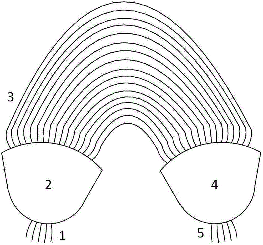
[0042] The size of the waveguide (including the array waveguide, the input and output waveguides) is 450nm, the ridge waveguide is used, and the etching depth is 130nm. Design a 1×4 arrayed waveguide grating with a center wavelength of 1565nm and a channel spacing of 8nm.
[0043] In this embodiment, the following planarization method is adopted:
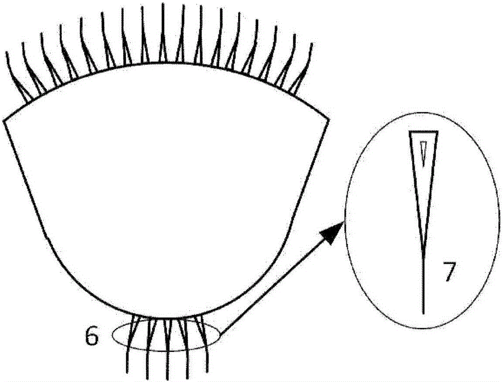
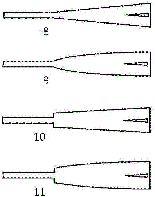
[0044] 1. Keep the original size unchanged, and add an exponentially changing tapered structure at the connection between the ridge waveguide (input / output waveguide and waveguide array) and the slab waveguide as a pre-broadening area. The pre-broadened region gen...
PUM
 Abstract
Description
Claims
Application Information


