Routing-free LED packaging structure and preparation method therefor

An LED packaging, wire-free technology, applied in electrical components, electric solid devices, circuits, etc., can solve the problems of complex preparation process, limited by wire bonding conditions and wire yield, and high cost, and achieves simple packaging process, Improve the yield of packaging products and enhance the effect of chip light-emitting

Inactive Publication Date: 2015-12-09
SHANDONG INSPUR HUAGUANG OPTOELECTRONICS
View PDF5 Cites 7 Cited by
  • Summary
  • Abstract
  • Description
  • Claims
  • Application Information

AI Technical Summary

Problems solved by technology

[0007] Aiming at the existing problems in the existing LED packaging process, such as complex preparation process, high cost, and limitation of welding wire conditions and yield rate, the present invention provides a wire-free LED packaging structure with simple packaging process and high yield rate, and at the same time A preparation method of the structure is provided

Method used


Image

  • Routing-free LED packaging structure and preparation method therefor
  • Routing-free LED packaging structure and preparation method therefor
  • Routing-free LED packaging structure and preparation method therefor

Examples


Embodiment Construction

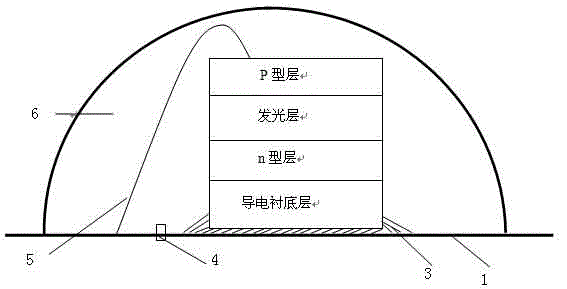
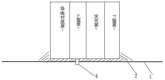
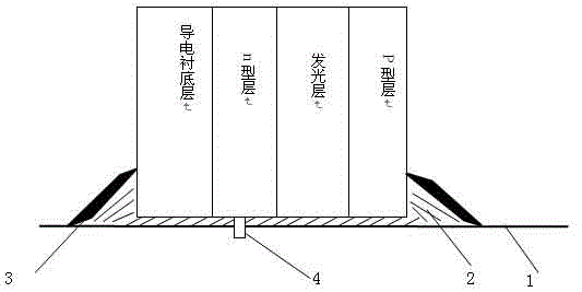
[0024] The wire-free LED packaging structure of the present invention is as follows: Figure 4 As shown, it includes an LED chip and a die-bonding substrate 1. The LED chip is placed sideways on the die-bonding substrate 1, and the two are bonded by insulating die-bonding glue 2. The side of the side-turned LED chip is also coated with insulating die-bonding. Glue, coating conductive silver glue 3 on both sides parallel to the direction of each conductive layer of the LED chip, the conductive silver glue 3 electrically connects the LED chip and the die-bonding substrate 1, and the die-bonding substrate 1 is provided with an insulating partition 4 to connect the The die-bonding substrate 1 is electrically disconnected to form positive and negative poles, which are respectively connected with the conductive silver glue 3 on the two sides of the LED chip. The package structure is suitable for LED chips with a vertical structure.

[0025] The preparation steps of the above-mentio...


PUM


Abstract

A routing-free LED packaging structure and a preparation method therefor are disclosed. The routing-free LED packaging structure comprises an LED chip and a die-bonding substrate; the LED chip is arranged on the die-bonding substrate in a side-down manner; the LED chip and the die-bonding substrate are glued through insulation die-bonding adhesive; the side face of the side-down LED chip is coated with the insulation die-bonding adhesive; conductive silver adhesive for enabling the LED chip and the die-bonding substrate to be electrically communicated is coated on the insulation die-bonding adhesive on the side face of the LED chip; the LED chip is arranged in the side-down manner; the LED chip is glued on the die-bonding substrate through the insulation die-bonding adhesive; meanwhile, the insulation die-bonding adhesive is coated on the periphery, the side faces and the bottom of the side-down LED chip and then the LED chip is roasted and cured; the conductive silver adhesive is dispensed on the insulation die-bonding adhesive on the side face of the LED chip and then the LED chip is roasted and cured; and the LED chip is wrapped with potting adhesive. According to the preparation method, the LED chip is arranged in the side-down manner, and then die-bonding for two times by the die-bonding glue is performed, so that the purpose of electrically communicating the chip with the die-bonding substrate is fulfilled, and meanwhile, the light-emitting of the chip is reinforced, the packaging process is simple and the yield of the packaged product is high.

Description

technical field [0001] The invention relates to an LED packaging structure and a preparation method thereof, belonging to the technical field of semiconductor light-emitting device manufacturing. Background technique [0002] The emergence of LED is a revolution for traditional light sources. LED is very popular in the lighting market due to its excellent characteristics, but it also brings the disadvantages of high cost, such as aluminum for heat dissipation and gold wire for packaging. The use of gold wire bonding in packaging engineering is bound to cause difficulties in cost control for the popularization of LEDs. [0003] The traditional LED chip solid-chip packaging structure is as follows: figure 1 As shown, the conductive substrate layer of the LED chip with the conductive substrate layer, the n-type layer, the light-emitting layer and the p-type layer from the bottom to the top is solidified on the solid crystal substrate 1 through the conductive silver glue 3, and...

Claims


Application Information

Patent Timeline
Patent Type & Authority Applications(China)
IPC IPC(8): H01L33/48H01L33/62H01L33/00
CPCH01L2224/29339H01L2224/48091H01L2224/73265H01L2224/83951H01L2924/00014H01L33/48H01L33/005H01L33/62H01L2933/0066
Inventor 于峰彭璐夏伟徐现刚
Owner SHANDONG INSPUR HUAGUANG OPTOELECTRONICS
Why Eureka
Try Eureka