Electrodes for semiconductor devices and methods of forming the same

A semiconductor and electrode technology, applied in the fields of semiconductor devices, semiconductor/solid-state device manufacturing, semiconductor/solid-state device components, etc., can solve the problem of difficulty in repeatedly manufacturing inclined field plates, etc., and achieve high breakdown voltage and low on-resistance. Effect

Active Publication Date: 2015-12-16
TRANSPHORM INC
View PDF4 Cites 15 Cited by
  • Summary
  • Abstract
  • Description
  • Claims
  • Application Information

AI Technical Summary

Problems solved by technology

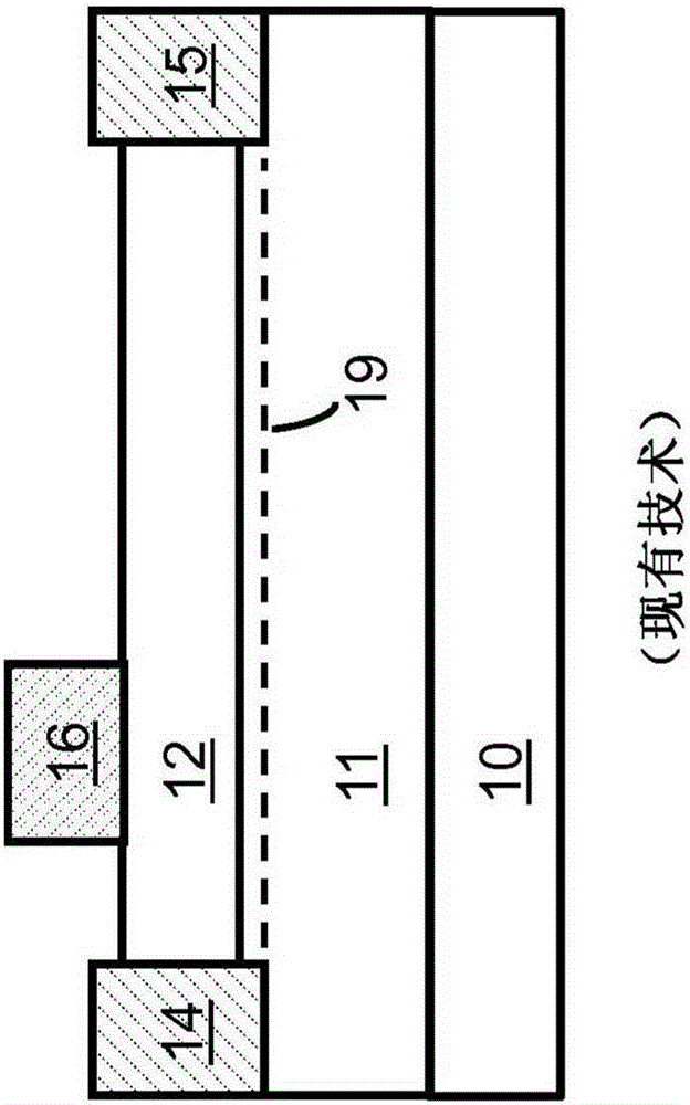
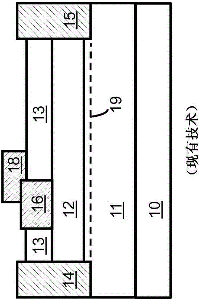
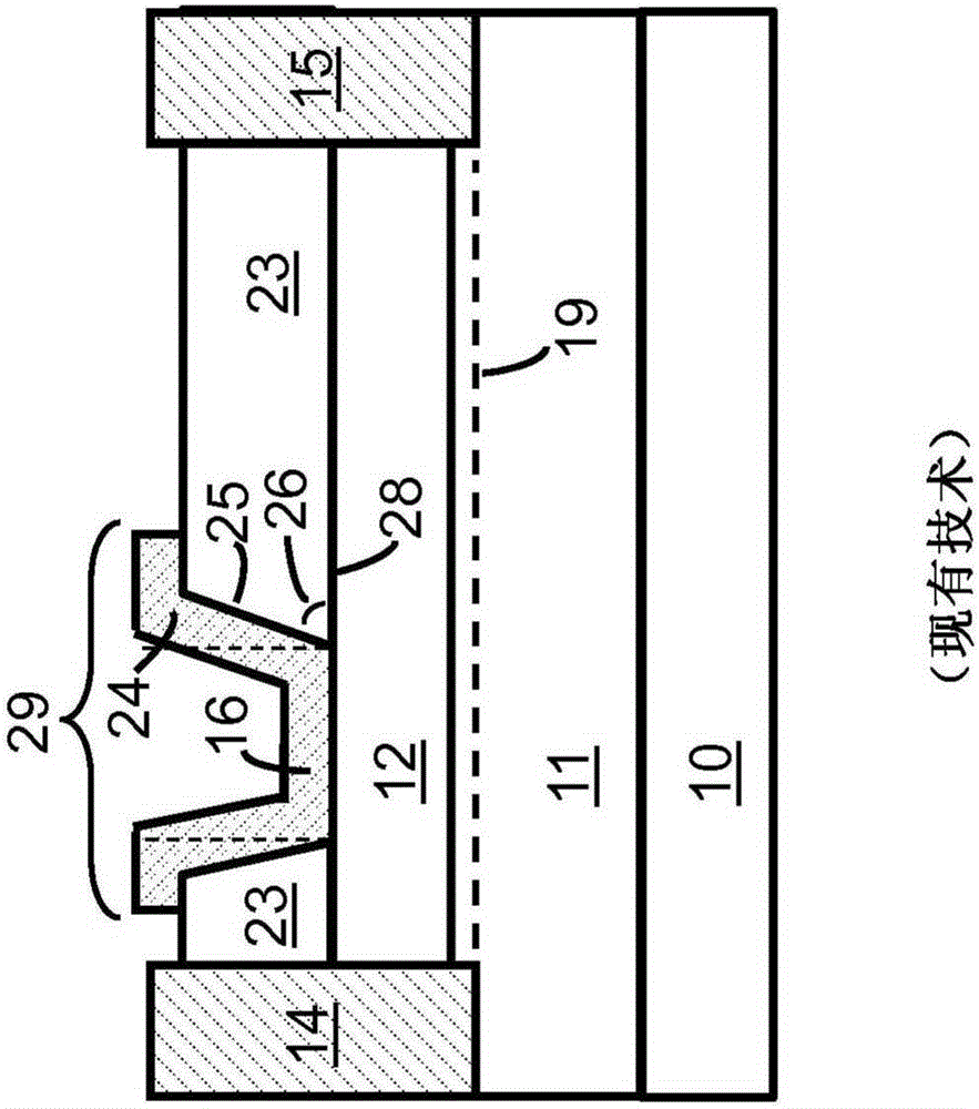
However, reducing the angle 26 results in a longer lateral extension of the field plate 24 towards the drain 15, which may require a larger spacin

Method used


Image

  • Electrodes for semiconductor devices and methods of forming the same
  • Electrodes for semiconductor devices and methods of forming the same
  • Electrodes for semiconductor devices and methods of forming the same

Examples


Embodiment Construction

[0027] Transistors based on III-N heterostructures are described. The electrodes of the device are designed such that the device is reproducible, supports high voltage and low leakage current, and exhibits low on-resistance and low gate capacitance. A method of forming the electrode is also described. The III-N devices described herein may be high voltage devices suitable for high voltage applications. In such a high-voltage transistor, when the transistor is biased off (that is, the voltage on the gate relative to the source is less than the threshold voltage of the transistor), it can support at least all source-drain voltages less than or equal to its High voltage in the application used, for example the high voltage may be 100V, 300V, 600V, 1200V, 1700V or higher. When a high-voltage transistor is biased on (that is, the voltage on the gate relative to the source is greater than the threshold voltage of the transistor), it can conduct large currents with a low turn-on vo...


PUM

PropertyMeasurementUnit
Thicknessaaaaaaaaaa

Abstract

An III-N semiconductor HEMT device includes an electrode-defining layer on a III-N material structure. The electrode-defining layer has a recess with a first sidewall proximal to the drain and a second sidewall proximal to the source, each sidewall comprising a plurality of steps. A portion of the recess distal from the III-N material structure has a larger width than a portion of the recess proximal to the III-N material structure. An electrode is in the recess, the electrode including an extending portion over the first sidewall. A portion of the electrode-defining layer is between the extending portion and the III-N material structure. The first sidewall forms a first effective angle relative to the surface of the III-N material structure and the second sidewall forms a second effective angle relative to the surface of the III-N material structure, the second effective angle being larger than the first effective angle.

Description

[0001] Cross References to Related Applications [0002] This application claims priority to US Provisional Patent Application No. 61 / 765,635, filed February 15, 2013. The disclosure of the prior application is considered a part of the disclosure of the present application and is incorporated by reference into the disclosure of the present application. technical field [0003] The present invention relates to semiconductor electronic devices and, in particular, to devices having electrodes connected to field plates. Background technique [0004] To date, modern power semiconductor diodes, such as high-voltage P-I-N diodes, and power transistors, such as power MOSFETs and insulated gate bipolar transistors (IGBTs), have generally been fabricated from silicon (Si) semiconductor materials. Recently, silicon carbide (SiC) power devices have been studied due to their excellent performance. III-nitride (III-N) semiconductor devices are now emerging as an attractive candidate to ...

Claims


Application Information

Patent Timeline
IPC IPC(8): H01L29/778H01L21/335
CPCH01L29/7787H01L21/28114H01L21/283H01L21/28581H01L21/28587H01L21/28593H01L21/76804H01L23/291H01L23/3171H01L29/045H01L29/0696H01L29/2003H01L29/205H01L29/402H01L29/41H01L29/41725H01L29/41766H01L29/42316H01L29/4236H01L29/42376H01L29/4238H01L29/66462H01L29/778H01L2924/0002H01L2924/00
Inventor 斯拉班缇·乔杜里乌梅什·米什拉尤瓦扎·多拉
Owner TRANSPHORM INC
Why Eureka
Try Eureka