Ultra-thick copper circuit board and manufacturing method thereof

A manufacturing method and circuit board technology, applied in printed circuit manufacturing, printed circuit, printed circuit, etc., can solve problems such as difficult performance guarantee and low product yield rate, and achieve reliable performance, simple manufacturing method, and improved yield rate.

Active Publication Date: 2015-12-23
GCI SCI & TECH
View PDF8 Cites 21 Cited by
  • Summary
  • Abstract
  • Description
  • Claims
  • Application Information

AI Technical Summary

Problems solved by technology

[0003] At present, most manufacturers can only produce thick copper circuit boards with a copper thickness of less than 6OZ. It is difficult to meet the production quality requirements for thick copper circuit boards above 8OZ. The product yield rate is low and the performance is difficult to guarantee.

Method used


Image

  • Ultra-thick copper circuit board and manufacturing method thereof
  • Ultra-thick copper circuit board and manufacturing method thereof
  • Ultra-thick copper circuit board and manufacturing method thereof

Examples


Embodiment 1

[0036] A kind of manufacturing method of the ultra-thick copper circuit board of present embodiment, comprises the following steps:

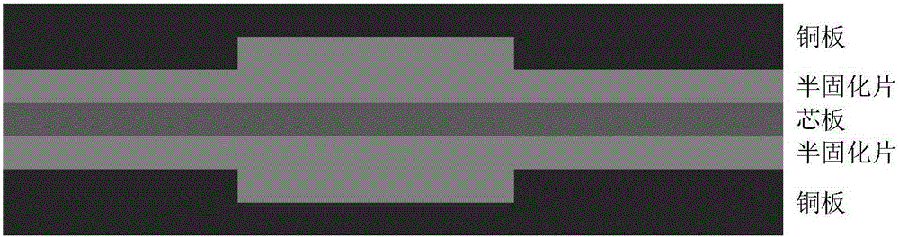
[0037] (1) The copper plate (thickness is 8OZ) is blanked, after drilling the positioning holes, the wet film printing operation is performed on the copper plate first, and after baking at 70-80°C for 20 minutes, the dry film is applied, and then the dry film is applied on the copper plate. On the first side, exposure and development expose the non-line pattern area, and the copper skin in the non-line pattern area of ​​the copper plate is etched away by 50% of the total copper plate thickness by etching to form a groove. The partially etched copper plate is as follows figure 1 As shown, then the copper plate is stripped and etched for inspection;

[0038] (2) Browning the core plate after blanking and the copper plate that step (1) obtains, filling epoxy resin powder in the groove of step (1) gained copper plate, the filling thickness of descri...

Embodiment 2

[0045] A kind of manufacturing method of the ultra-thick copper circuit board of present embodiment, comprises the following steps:

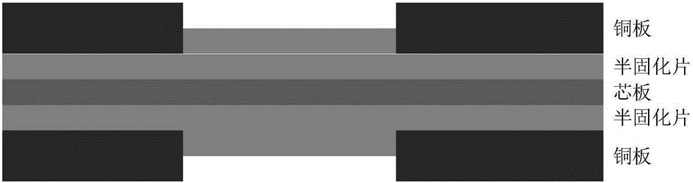
[0046] (1) The copper plate (thickness is 16OZ) is blanked, after drilling the positioning hole, the wet film printing operation is performed on the copper plate, and after baking at 70-80°C for 30 minutes, the dry film is applied, and then the copper plate is printed. On the first side, after exposure and development, the non-circuit pattern area is exposed, and the copper skin in the non-circuit pattern area of ​​the copper plate is etched away by 40% of the total copper plate thickness by etching to form a groove, and then the copper plate is subjected to film removal and etching inspection;

[0047] (2) Carry out browning to the copper plate that core plate and step (1) obtain after blanking, fill in the epoxy resin powder in the groove of described copper plate in step (1), the filling thickness of described epoxy resin powder is 1 / 2 of the...

Embodiment 3

[0053] A kind of manufacturing method of the ultra-thick copper circuit board of present embodiment, comprises the following steps:

[0054] (1) The copper plate (thickness is 28OZ) is blanked, after drilling the positioning hole, the wet film printing operation is performed on the copper plate first, and after baking at 70-80°C for 40 minutes, the dry film is applied, and then the copper plate is printed. On the first side, after exposure and development, the non-circuit pattern area is exposed, and the copper skin in the non-circuit pattern area of ​​the copper plate is etched away by 60% of the total copper plate thickness by etching to form a groove, and then the copper plate is subjected to film removal and etching inspection;

[0055] (2) Carry out browning to the copper plate that core plate and step (1) obtain after blanking, fill in the epoxy resin powder in the groove of described copper plate in step (1), the filling thickness of described epoxy resin powder is 1 / 2 ...


PUM


Abstract

The invention relates to an ultra-thick copper circuit board and a manufacturing method thereof. The manufacturing method comprises the following steps: (1) etching partial thickness of a non-circuit-pattern area copper plate on one side of the copper plate by adopting an etching process to form a groove, and carrying out the lamination step on the side by virtue of a binding layer; (2) drilling, metalizing the hole, etching the rest thickness of the non-circuit-pattern area copper plate on the other side of the copper plate by adopting the etching process to obtain a circuit pattern; (3) carrying out the printing resistance soldering steps: printing resin onto the non-circuit-pattern area, drying, and then printing ink onto the entire circuit board; and (4) carrying out the subsequent procedures. By adopting the method, the copper plate of 80Z or more is realized, and the blank that a multilayer ultra-thick copper circuit board cannot be manufactured in the industry is filled; moreover, the manufacturing method is simple, the manufacturing method can be realized by adopting a circuit board conventional device, and the manufactured ultra-thick copper circuit board is good in yield and reliable in performance.

Description

technical field [0001] The invention relates to the field of circuit board manufacturing, in particular to an ultra-thick copper circuit board and a manufacturing method thereof. Background technique [0002] With the development of PCB (Printed Circuit Board, printed circuit board) in the direction of small size, light weight, three-dimensional installation and high connection reliability, the demand for ultra-thick copper circuit boards is increasing, and it has become one of the main growth points of circuit board manufacturing. [0003] At present, most manufacturers can only produce thick copper circuit boards with a copper thickness of less than 6OZ. It is difficult to meet the production quality requirements for thick copper circuit boards above 8OZ. The yield rate of products is low and performance is difficult to guarantee. Contents of the invention [0004] Based on this, it is necessary to provide an ultra-thick copper circuit board with high yield rate and reli...

Claims


Application Information

Patent Timeline
Patent Type & Authority Applications(China)
IPC IPC(8): H05K3/02H05K3/06
CPCH05K3/022H05K3/06H05K2201/098
Inventor 吴传亮任代学李超谋黄德业
Owner GCI SCI & TECH
Why Eureka
Try Eureka