Super-high-density LED display device and manufacturing method thereof

A display device, ultra-high-density technology, applied in the direction of electric solid-state devices, semiconductor devices, instruments, etc., can solve the problems of increased packaging costs, color drift, light decay and inconsistent voltage drift characteristics, to prevent light diffusion and improve resolution Effect of Ratio and Contrast

Pending Publication Date: 2015-12-30
NANJING UNIV
View PDF8 Cites 18 Cited by
  • Summary
  • Abstract
  • Description
  • Claims
  • Application Information

AI Technical Summary

Problems solved by technology

[0004] 1. The point light source components of the LED display are assembled on the substrate by SMD or in-line LED devices. A single point light source has a large volume and a large pixel pitch. To achieve a pixel pitch of less than 1mm, the SMD device package The requirements are higher, and the packaging cost is greatly increased, which is not conducive to the wide application of LED display in the field of digital and micro display.
[0005] 2. LED chips with different semiconductor materials are used for each pixel, and their light decay and voltage drift characteristics are inconsistent, so that color drift occurs during use and affects the display effect of the screen image

Method used


Image

  • Super-high-density LED display device and manufacturing method thereof
  • Super-high-density LED display device and manufacturing method thereof
  • Super-high-density LED display device and manufacturing method thereof

Examples


Embodiment 1

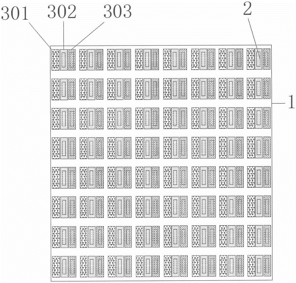
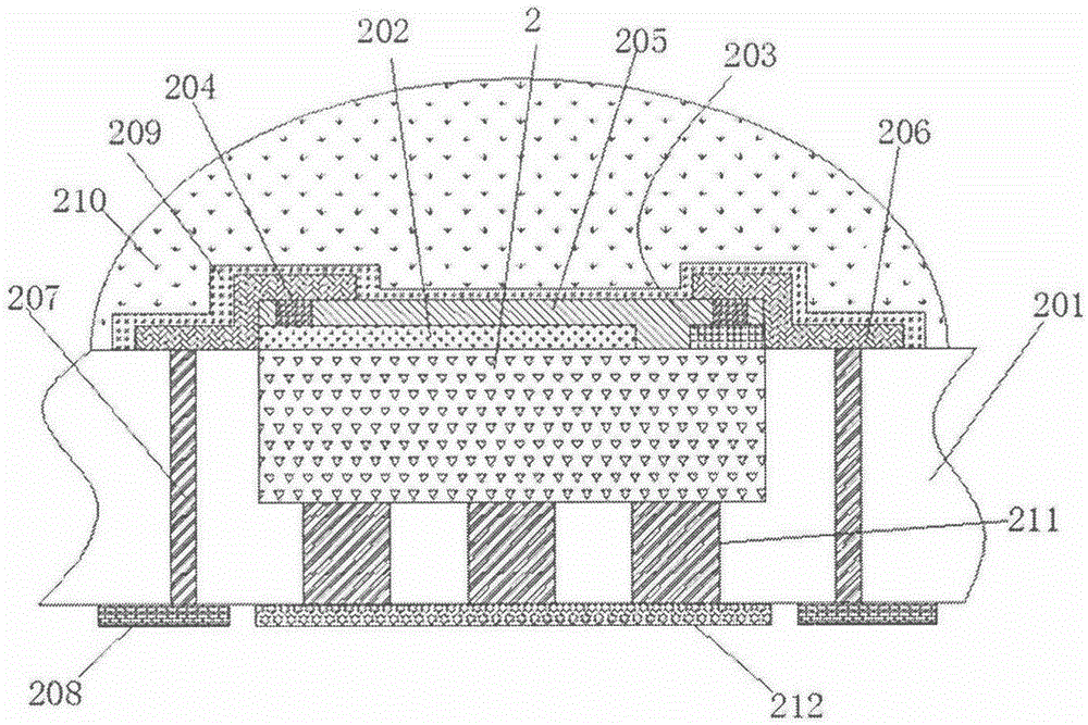
[0041] see figure 1 , which is a schematic diagram of the ultra-high-density LED display device of the present invention, including 8x8 pixels, and each pixel is composed of 3 units, wherein 1 is a substrate, 2 is an LED light-emitting chip, 301, 302 and 303 are red, 303, respectively. Green and blue light conversion materials. see figure 2 , figure 2 It is a schematic structural diagram of an LED chip in a unit in a single pixel according to Embodiment 1 of the present invention, and the LED chip array adopts a fan-out wafer-level packaging form. 201 is a molding compound, 2 is an LED chip, the surface of the LED chip is provided with a P-type ohmic contact layer 202 and an N-type ohmic contact layer 203, and the metal electrodes 204 are respectively arranged on the surfaces of the P-type ohmic contact layer 202 and the N-type ohmic contact layer 203, The passivation layer 205 is arranged between and next to the two electrodes to avoid the short circuit problem caused by...

Embodiment 2

[0064] see Figure 4 , Figure 4 It is a structural schematic diagram of a flip-chip LED chip on a substrate according to Embodiment 2 of the present invention. Figure 4 It is a schematic structural diagram of an LED chip in a unit in a single pixel according to Embodiment 2 of the present invention, and the LED chip array adopts a flip-chip packaging form. 401 is the substrate, on the surface of the LED chip 2, a P extremely high reflective layer 402 and an N extremely high reflective layer 403 are set, metal electrodes 404 are respectively set on the surface of the high reflective layer, and a passivation layer 405 is set between and next to the two metal electrodes , to avoid the short-circuit problem caused by the direct contact of the two metal electrodes, the double wiring layers 408 and 410 are arranged on the surface of the substrate 401, and the under-bump metal layer 407 is arranged on the metal wiring layer 408, and the solder ball bump 406 is used for For connec...

Embodiment 3

[0088] see Figure 5 , Figure 5 It is a schematic structural diagram of an LED chip according to Embodiment 3 of the present invention, and the LED chip array adopts a fan-out wafer-level packaging form. 201 is a molding compound, 2 is an LED chip, the surface of the LED chip is provided with a P-type ohmic contact layer 202 and an N-type ohmic contact layer 203, and the metal electrodes 204 are respectively arranged on the surfaces of the P-type ohmic contact layer 202 and the N-type ohmic contact layer 203, The passivation layer 205 is arranged between the two electrodes to avoid the short circuit problem caused by the direct contact between the two electrodes, the metal wiring layer 206 is arranged on the surface of the metal electrode, and the through hole 207 is arranged inside the molding compound for the connection between the light-emitting chip and the external driving circuit. For connection, the other side of the molding compound opposite to the light-emitting chi...


PUM


Abstract

The invention discloses a super-high-density LED display device which comprises a substrate and an LED chip array packaged on the substrate. The chip array comprises a plurality of LED chips distributed evenly at intervals. By means of the Fan-Out Wafer-Level Package (FOWLP) process, the packaging area is narrowed, and the resolution ratio of an LED display screen is increased; all the LED chips are the same in structure, light-emitting wave band and type, the LED chips emit red light, green light and blue light after being coated with red light fluorescent powder, green light fluorescent powder and blue light fluorescent powder in a chip light-emitting curing mode respectively, and therefore it is ensured that the LED chips are consistent in light attenuation in the use process, and the development performance of the display screen is improved; pixel point distances can be smaller than 1 mm and even smaller than 0.1 mm, better performance such as high integrity, high resolution and consistent light color of the LED display device is achieved, and the super-high-density LED display device is importantly applied to indoor high-density display screens, projection devices and wearable display devices.

Description

technical field [0001] The invention relates to the technical field of LED display, in particular to an ultra-high-density LED display device. Background technique [0002] LED display devices are mainly composed of LED dot matrix. By controlling the on and off of various LEDs, such as red, blue, white, and green LEDs, it can display text, graphics, images, animations, market prices, videos, video signals, etc. display screen for various information. Due to the low working voltage of the LED (only 1.5-3.6V), it can actively emit light and have a certain brightness, and the brightness can be adjusted by voltage (or current). Among display devices, there is no other display method that can match the LED display method. [0003] However, existing LED technology display screens have the following defects: [0004] 1. The point light source components of the LED display are assembled on the substrate by SMD or in-line LED devices. A single point light source has a large volume...

Claims


Application Information

Patent Timeline
Patent Type & Authority Applications(China)
IPC IPC(8): H01L27/15G09F9/33
CPCH01L27/156G09F9/33
Inventor 周玉刚王小莉张荣
Owner NANJING UNIV
Why Eureka
Try Eureka