Check patentability & draft patents in minutes with Patsnap Eureka AI!

VDMOS structure of super junction terminal

A technology of junction terminal and terminal area, which is applied in the field of semiconductor devices to achieve the effects of reducing cost, reducing on-resistance, and improving withstand voltage

Inactive Publication Date: 2015-12-30
ZHANGJIAGANG EVER POWER SEMICON
View PDF4 Cites 3 Cited by
  • Summary
  • Abstract
  • Description
  • Claims
  • Application Information

AI Technical Summary

Problems solved by technology

Therefore, the blocking capability of the superjunction is very sensitive to the charge imbalance between the P-type semiconductor pillars and the N-type semiconductor pillars, which brings great challenges and risks to device fabrication.

Method used


Image

  • VDMOS structure of super junction terminal
  • VDMOS structure of super junction terminal

Examples


Embodiment 1

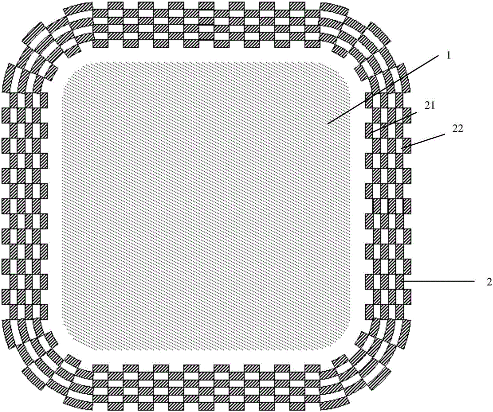
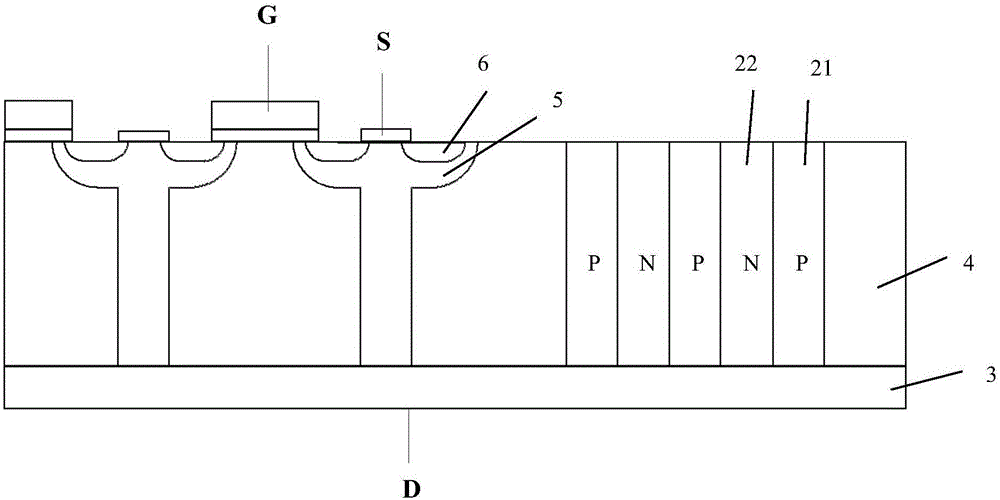
[0016] Such as figure 1 As shown, the VDMOS structure of the present invention is divided into two parts, the active region 1 and the terminal region 2. The terminal region 2 surrounds the active region 1, wherein the active region 1 can be a planar structure, a trench structure or a super junction structure. The terminal area 2 of the present invention is provided with P-type semiconductor columns 21 and N-type semiconductor columns 22, wherein the P-type semiconductor columns 21 and N-type semiconductor columns 22 are not only alternately arranged in the width direction of the terminal area 2, but also alternately arranged in the length direction of the terminal area 2 arrangement.

[0017] In this embodiment, the active region 1 takes a super junction structure as an example, such as figure 2 As shown, it is a cross-sectional structure of the present invention, and its structure is to grow a lightly doped N-drift region on an N+ silicon substrate, and to dig trenches in t...


PUM


Abstract

The invention relates to the technical field of a semiconductor device, especially to a VDMOS structure of a super junction terminal. The VDMOS structure comprises a silicone substrate and a drift region arranged on the silicone substrate; the drift region comprises an active region and a terminal region surrounding the active region, the active region is provided with a well region and a source region, and the terminal region is provided with P type and N type semiconductor columns, which are arranged alternatively, in both the width and length directions; and the active region in the upper surface of the substrate silicon is provided with a grid G and a source S, and the lower surface of the silicon substrate is provided with a drain D. The VDMOS structure has the advantages that the super junction structure can effectively coordinate relation between the breakdown voltage and the ON resistance, the P type and N type semiconductor columns are alternatively arranged in the width and length directions of the terminal region to achieve charge balance more effectively, the withstand voltage is improved, the ON resistance is reduced, the area of the terminal region is reduced, the chip area is further reduced, and the cost is reduced.

Description

technical field [0001] The invention relates to the technical field of semiconductor devices, in particular to a super junction terminal VDMOS structure. Background technique [0002] VDMOS (Vertical Double Diffused Metal-Oxide Semiconductor Field Effect Transistor) is widely used in power electronic systems. In ideal off-state conditions, it can withstand high voltage, and has a small voltage drop when it is turned on. The current density is high, and the switching speed is fast, and the switching loss is small. However, ideal performance is often not achieved in practice. In the field of high-voltage applications, the traditional VDMOS needs to increase the thickness of the drift region and reduce the doping concentration of the epitaxial layer to increase the breakdown voltage, which will inevitably increase the on-resistance of the device and increase power consumption. The superjunction concept is based on achieving charge balance in the off state, and uses overlappin...

Claims


Application Information

Patent Timeline
IPC IPC(8): H01L29/78H01L29/06
CPCH01L29/7802H01L29/06H01L29/0607H01L29/0611
Inventor 周炳石英学张志娟郝建勇
Owner ZHANGJIAGANG EVER POWER SEMICON
Features
  • R&D
  • Intellectual Property
  • Life Sciences
  • Materials
  • Tech Scout
  • Unparalleled Data Quality
  • Higher Quality Content
  • 60% Fewer Hallucinations
Learn More