Optical waveguide detector capable of eliminating parasitic capacitance

A technology of parasitic capacitance and optical waveguide, which is applied in the direction of semiconductor devices, circuits, electrical components, etc., can solve the problems of small waveguide layer thickness, large total capacitance, large cross-sectional area and distance, etc., to improve response bandwidth and reduce total capacitance , Improve the effect of electrical conductivity

Inactive Publication Date: 2015-12-30
UNIV OF ELECTRONICS SCI & TECH OF CHINA
View PDF3 Cites 2 Cited by
  • Summary
  • Abstract
  • Description
  • Claims
  • Application Information

AI Technical Summary

Problems solved by technology

[0007] Current optical waveguide detectors such as image 3 As shown, the n-electrode is located on the substrate and is in contact with the waveguide layer at the same time. However, due to the small thickness of the waveguide layer, the contact area is very small. In order to increase the contact area and allow a larger current to flow, it is necessary to It is heavily doped to make it have good conductivity; thus, a parasitic capacitance is generated between the p-electrode of the detector and the substrate, and the parasitic capacitance is in parallel with the junction capacitance. Compared with the junction capacitance, the cross-sectional area of ​​the parasitic capacitance and The distance is relatively large, and the capacitive effect cannot be ignored, resulting in a large total capacitance, which limits the response bandwidth of the optical waveguide detector.

Method used


Image

  • Optical waveguide detector capable of eliminating parasitic capacitance
  • Optical waveguide detector capable of eliminating parasitic capacitance
  • Optical waveguide detector capable of eliminating parasitic capacitance

Examples


Embodiment Construction

[0024] The present invention will be further elaborated below in conjunction with the accompanying drawings and specific embodiments.

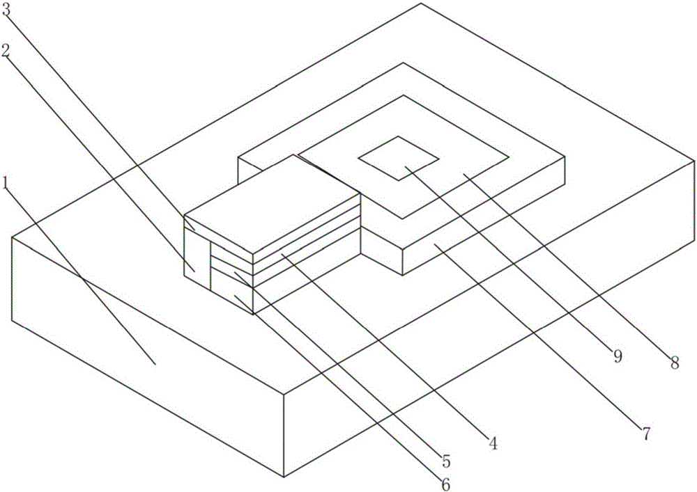
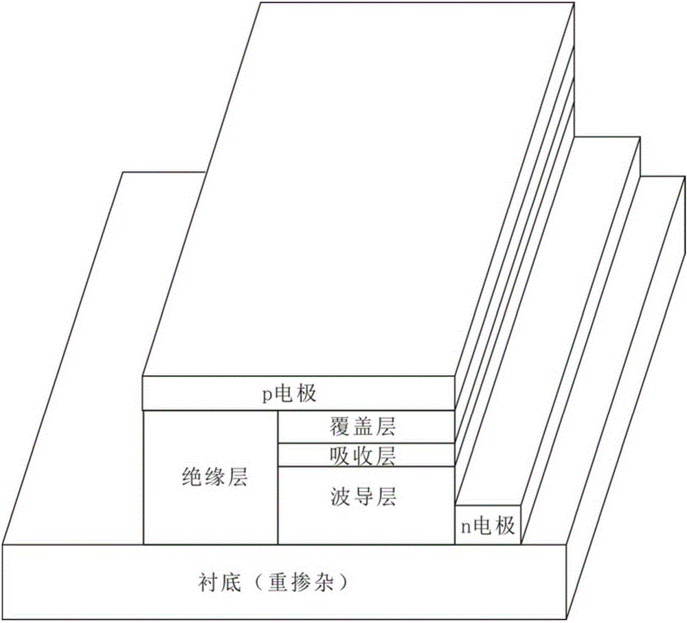
[0025] Such as figure 1 As shown, the optical waveguide detector for eliminating parasitic capacitance of the present invention comprises a substrate 1, an insulating layer-2, a p-electrode 3, a cover layer 4, an absorption layer 5 and a waveguide layer-6, and the insulating layer-2 is placed on the substrate 1, one side of the waveguide layer 6 is in contact with one side of the insulating layer 2, and placed on the substrate 1 at the same time, the absorbing layer 5 is placed on the waveguide layer 6, and one side of the absorbing layer 5 is in contact with one side of the insulating layer 2 , the cover layer 4 is placed on the absorber layer 5, one side of the cover layer 4 is in contact with the insulating layer 2, and the top height of the cover layer 4 is consistent with that of the insulating layer 2, and the p-electrode 3 is placed be...


PUM


Abstract

The invention discloses an optical waveguide detector capable of eliminating parasitic capacitance. The optical waveguide detector includes a waveguide layer 2, an insulating layer 2 and an n electrode; the waveguide layer 2 is a rectangular body of which the middle is hollowed out; one edge of the waveguide layer 2 contacts with a waveguide layer 1 and an insulating layer 1; the insulating layer 2 is a rectangular body of which the middle is hollowed out; the bottom of the insulating layer 2 contacts with the waveguide layer 2; the four walls of the insulating layer 2 contacts with the inner walls of the waveguide layer 2; the n electrode is arranged at the center of the insulating layer 2; and the bottom of the n electrode contacts with the waveguide layer 2. According to the optical waveguide detector of the invention, the n electrode is shifted to behind at rear flat stage, and the n electrode does not contact with a substrate any more, and at the same time, the substrate does not need heavy doping for improving conductivity, and therefore, parasitic capacitance is no longer generated between a p electrode and the substrate, and total capacitance can be reduced, and thus, the response bandwidth of the optical waveguide detector can be improved.

Description

technical field [0001] The invention belongs to the field of optoelectronics, in particular to an optical waveguide detector capable of eliminating parasitic capacitance. Background technique [0002] A high-power high-speed photodetector is a detection device based on the interaction between light and matter, and its function is to convert the incident light signal into a high-power high-frequency signal. High-power high-speed optical detector is an indispensable device in optically controlled phased array radar, ultra-high-speed test system and optical fiber LAN communication, and its performance plays a decisive role in the whole system. [0003] Conventional vertical-incidence photodetectors cannot meet both high-speed and high-power requirements. The main reasons are as follows: one is the saturation effect, which limits the photocurrent; the other is the long transit time, which limits the response frequency; the third is that the light absorption of the intrinsic lay...

Claims


Application Information

Patent Timeline
Patent Type & Authority Applications(China)
IPC IPC(8): H01L31/0232H01L31/0224
CPCH01L31/022408H01L31/02327
Inventor 余学才马朝阳李林松
Owner UNIV OF ELECTRONICS SCI & TECH OF CHINA
Why Eureka
Try Eureka