Photoelectric detector and preparation method thereof

A photodetector and electrode technology, applied in circuits, electrical components, semiconductor devices, etc., can solve the problems of increased dark current of detectors, large coupling loss of direct coupling, etc., to achieve large response bandwidth, improve performance, and improve coupling efficiency Effect

Active Publication Date: 2021-03-26
INST OF MICROELECTRONICS CHINESE ACAD OF SCI
View PDF5 Cites 1 Cited by
  • Summary
  • Abstract
  • Description
  • Claims
  • Application Information

AI Technical Summary

Problems solved by technology

[0003] Efficient optical coupling and transmission is the key to the reliable application of optoelectronic devices, but in waveguide detectors, due to the mode mismatch between the waveguide and the germanium layer absorption region, there is a large coupling loss in direct coupling
At the same time, due to the interface defects between the silicon layer and the germanium layer, if the absorption region of the germanium layer is too long, the dark current of the detector will increase significantly.

Method used


Image

  • Photoelectric detector and preparation method thereof
  • Photoelectric detector and preparation method thereof
  • Photoelectric detector and preparation method thereof

Examples


Embodiment 1

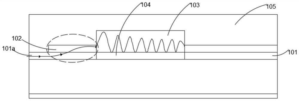
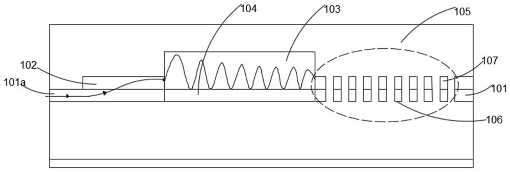
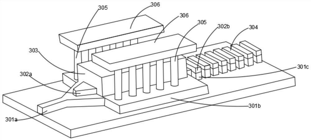
[0051] Such as image 3 Horizontal photodetectors shown, including:

[0052] SOI substrate, one end of the top layer of silicon forms a pyramid-shaped silicon waveguide 301a, and the opposite end forms a Bragg grating array 304, and each grating in the array is formed by stacking top-layer silicon 301c and polysilicon 302b from bottom to top; the pyramid-shaped silicon waveguide 301a has a first end and a second end, the area of ​​the first end being smaller than the area of ​​the second end.

[0053] The upper surface of the silicon waveguide 301a close to the first end is covered with a pyramid-shaped polysilicon 302a, and the polysilicon 302a is used to buffer the coupling of the silicon waveguide 301a to the germanium layer 303 .

[0054] The upper surface of the silicon waveguide 301a close to the second end is covered with a germanium layer 303, and the germanium layer 303 is spliced ​​together with the aforementioned polysilicon 302a.

[0055] A P-doped region 301b an...

Embodiment 2

[0068] Utilize the method similar to embodiment 1 to make vertical type photodetector, structure such as Figure 12 As shown (cross-sectional view along the waveguide direction), the difference between the two manufacturing methods is that the implanted ion regions are different (the N-doped region 401 is arranged on the top-layer silicon, the silicon waveguide is still located on the top-layer silicon, and the P-doped region 403a is arranged on the germanium layer. 403 , the positions of the N-doped region and the P-doped region can also be exchanged in practical applications), and the position of the contact hole 404 changes accordingly.


PUM


Abstract

The invention relates to a photoelectric detector and a preparation method thereof. The photoelectric detector is of a transverse PN junction structure or a longitudinal PN junction structure, and comprises a semiconductor substrate provided with top-layer silicon, wherein a cone-shaped silicon waveguide is formed on the top silicon, the cone-shaped silicon waveguide is provided with a first end and a second end, and the area of the first end is smaller than that of the second end; the upper surface, close to the first end, of the silicon waveguide is covered with a first polycrystalline silicon layer; the upper surface, close to the second end, of the silicon waveguide is covered with a germanium layer, and the germanium layer and the first polycrystalline silicon layer are spliced together; wherein the P doped region and the N doped region are arranged in the top silicon layer and/or the germanium layer; and electrodes respectively formed on the upper surfaces of the P-doped region and the N-doped region. The coupling structure of the germanium-silicon photoelectric detector input waveguide active absorption region is optimized, high-efficiency coupling of the germanium-silicon photoelectric detector input waveguide active absorption region and the germanium-silicon photoelectric detector can be achieved, response is improved, and device power consumption is reduced.

Description

technical field [0001] The invention relates to the field of semiconductors, in particular to a photodetector and a preparation method thereof. Background technique [0002] Photodetectors are an important part of photonic integrated chips. Compared with the surface incidence detector, the waveguide detector can greatly increase the absorption length under the premise of maintaining the thickness of the absorbing layer. The propagation and absorption of light are along the direction of the waveguide, while the carrier transport is along the perpendicular direction. The direction can significantly improve the response speed and obtain high internal quantum efficiency; at the same time, the device area is smaller and the dark current is relatively low, which can significantly improve the noise and improve the sensitivity of the device. Therefore, photodetectors with this structure have attracted extensive attention. [0003] Efficient optical coupling and transmission is the...

Claims


Application Information

Patent Timeline
Patent Type & Authority Applications(China)
IPC IPC(8): H01L31/0232H01L31/109H01L31/18
CPCH01L31/02327H01L31/109H01L31/1804Y02P70/50
Inventor 李彬李志华唐波张鹏杨妍刘若男
Owner INST OF MICROELECTRONICS CHINESE ACAD OF SCI
Why Eureka
Try Eureka