Two-position SONOS memory and compiling, erasing and reading methods thereof

A memory and storage bit technology, applied in static memory, read-only memory, information storage, etc., can solve the problems of slow reading, writing, erasing, complex circuit structure, and high reliability requirements, and achieve low compilation current. , Solve the effect of complex circuit structure, increase storage density and storage capacity

Active Publication Date: 2016-01-06
SHANGHAI HUALI MICROELECTRONICS CORP
View PDF5 Cites 8 Cited by
  • Summary
  • Abstract
  • Description
  • Claims
  • Application Information

AI Technical Summary

Problems solved by technology

[0016] The purpose of the present invention is to overcome the above-mentioned defects existing in the prior art, provide a double-bit SONOS memory and its compiling, erasing and reading methods, which can solve the problem of high power consumption d

Method used


Image

  • Two-position SONOS memory and compiling, erasing and reading methods thereof
  • Two-position SONOS memory and compiling, erasing and reading methods thereof
  • Two-position SONOS memory and compiling, erasing and reading methods thereof

Examples


Embodiment Construction

[0045] The specific embodiment of the present invention will be further described in detail below in conjunction with the accompanying drawings.

[0046] It should be noted that, in the following specific embodiments, when describing the embodiments of the present invention in detail, in order to clearly show the structure of the present invention for the convenience of description, the structures in the drawings are not drawn according to the general scale, and are drawn Partial magnification, deformation and simplification are included, therefore, it should be avoided to be interpreted as a limitation of the present invention.

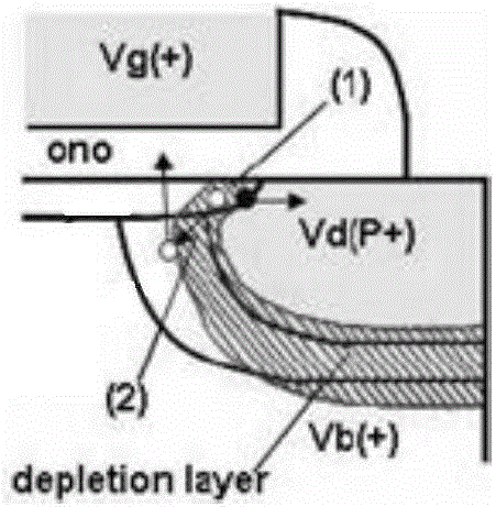
[0047] In the following specific embodiments of the present invention, please refer to figure 2 , figure 2 It is a structural schematic diagram of a dual-bit SONOS memory in a preferred embodiment of the present invention. Such as figure 2 As shown, a dual-bit SONOS memory of the present invention includes: a P-type silicon substrate 1 and a ga...


PUM

PropertyMeasurementUnit
Thicknessaaaaaaaaaa
Thicknessaaaaaaaaaa
Thicknessaaaaaaaaaa

Abstract

The invention discloses a two-position SONOS memory. The two-position SONOS memory comprises a P-type silicon substrate and a gate structure arranged on the substrate and between a source end and a drain end, wherein the substrate is provided with the N-type doped source end, the drain end and an N channel; and the gate structure successively comprises a first silicon dioxide layer, a silicon nitride layer, a second silicon dioxide layer and a polycrystalline silicon control gate from down to up, and the silicon nitride layer comprises a first storage position close to the drain end side and a second storage position close to the source end side and is used for storing charges. Low-power band-to-band tunneling hot hole injection compiling and channel FN electron tunneling erasing modes are adopted, and a back gate bias is utilized for assisting hot hole injection, so that a conventional SONOS device is smaller in gate length, and the problem of high power of existing channel hot electron injection compiling is solved; in addition, the two-position storage SONOS memory is higher in storage density and storage capacity, so that the two-position storage SONOS memory has great advantages in the market where large-capacity memories are popular at present.

Description

technical field [0001] The present invention relates to the technical field of semiconductor memory, more specifically, to a double-bit SONOS memory and methods for compiling, erasing and reading it. Background technique [0002] For the NOR flash memory unit, the most important factor limiting the further reduction of its size is the further shortening of the gate length. This is mainly because the compilation method of channel hot electron (CHE) injection used in NOR flash memory cells requires a certain voltage at the drain of the device, and this voltage has a great impact on the penetration of the source and drain. Therefore, channel hot electron (CHE) injection is not suitable for short-channel devices. Another problem is that NOR flash memory is limited by the programming rate compared with NAND and AND data storage devices. According to the prediction of the document "G. Servalli, et al., IEDMTech. Dig., 35_1, 2005", the physical limit of the gate length reduction ...

Claims


Application Information

Patent Timeline
IPC IPC(8): H01L27/115H01L29/423G11C16/04
Inventor 顾经纶
Owner SHANGHAI HUALI MICROELECTRONICS CORP
Why Eureka
Try Eureka