GaAs-based LED chip cutting method

A technology of LED chips and cutting methods, which is applied to fine working devices, electrical components, circuits, etc., can solve problems such as chip chipping and cracked tube cores, and achieve the effect of improving the appearance quality

Active Publication Date: 2016-01-06
SHANDONG INSPUR HUAGUANG OPTOELECTRONICS
View PDF9 Cites 33 Cited by
  • Summary
  • Abstract
  • Description
  • Claims
  • Application Information

AI Technical Summary

Problems solved by technology

[0009] Aiming at the problems that the current chip cutting technology is prone to chip chipping and cracking of the tube core, the invention provides a cutting method for GaAs-based LED chips that can avoid chipping and cracking of the tube core and improve the appearance quality after cutting

Method used


Image

  • GaAs-based LED chip cutting method
  • GaAs-based LED chip cutting method
  • GaAs-based LED chip cutting method

Examples


Embodiment Construction

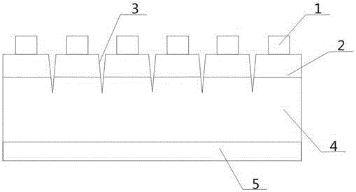
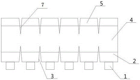
[0031] The cutting method of the GaAs-based LED chip of the present invention specifically comprises the following steps:

[0032] (1) Full half-cut on the P side

[0033] Place the electrode 1 of the P side of the LED chip upwards on the workbench of the saw blade, select the half-cut operation program and click "automatic cutting", the saw blade machine will automatically calibrate the level and start cutting until the CH1 and CH2 sides of the chip are cut. Such as figure 1 shown. Full half-cutting is first performed along the direction perpendicular to the large cleavage side of the chip, and then full-scale half-cutting is performed along the direction parallel to the large cleavage side to form criss-cross cutting grooves to separate the P-side electrodes 1 of the chip at equal intervals.

[0034] The initial feed speed of cutting is 10mm / s. After cutting 25 knives, the knife speed can be adjusted to 20-70mm / s according to the cutting conditions. 550-600μm. The half-c...


PUM

PropertyMeasurementUnit
thicknessaaaaaaaaaa
widthaaaaaaaaaa

Abstract

The invention discloses a GaAs-based LED chip cutting method. The method comprises the following steps: (1) semi-cutting is carried out on a P surface, criss-cross cutting grooves are formed, and chip P surface electrodes are separated at equal intervals; (2) the chip P electrodes face a white film downwardly, N electrodes face upwardly and are attached to the white film; (3) chip N surface scribing is carried out along the cutting grooves formed by P surface semi-cutting, and chip N surface stress is relieved; (4) film inverting is carried out on the scribed chip, and the chip is transferred to a blue film from the white film; and (5) on the chip N surface, a bonding tool of a chip breaking machine is used for chip breaking along scratches, and the chip is processed into independent crystal grains. The improved surface mount method is used, a cutting method which combines advantages of a chip sawing machine and a laser chip scribing machine is adopted, the chip P surface stress and the N surface stress are relieved maximally, deformation stress effects caused by film laminating can be reduced and edge collapse and pipe core breaking phenomena after the chip is cut are reduced, and the appearance quality after the chip is cut is improved.

Description

technical field [0001] The invention relates to a method for cutting LED (light emitting diode) chips, which belongs to the technical field of LED chip cutting. Background technique [0002] In the LED chip manufacturing process, dicing is the process of dividing the entire chip after photolithography, coating, thinning and other processes into single grains of the required size, which is indispensable in the semiconductor light-emitting diode chip manufacturing process. a process. For LED chips, the more traditional and the most widely used cutting method in the industry is saw blade cutting. [0003] Saw blade cutting is to use a high-speed rotating (3-4r / min) diamond knife to completely saw the chip into a single grain according to the program set according to the process requirements. The cutting method of the conventional GaAs-based LED chip is to use a diamond knife to micro-cut (half-cut) the chip, and then use a diamond knife to completely cut along the half-cut kn...

Claims


Application Information

Patent Timeline
Patent Type & Authority Applications(China)
IPC IPC(8): H01L33/00H01L21/78B28D5/00
CPCB28D5/00H01L21/78H01L33/0062
Inventor 郑军李法健齐国健刘琦徐现刚
Owner SHANDONG INSPUR HUAGUANG OPTOELECTRONICS
Why Eureka
Try Eureka