Manufacturing method of GaN-based light emitting diode

A technology of light-emitting diodes and manufacturing methods, which is applied in the direction of electrical components, circuits, semiconductor devices, etc., can solve the problems of high material cost and production cost, and long production time of light-emitting diodes, so as to reduce material costs and production costs, and reduce photolithography. The effect of reducing the number of times and reducing the production time

Active Publication Date: 2016-01-13
EPITOP PHOTOELECTRIC TECH
View PDF3 Cites 9 Cited by
  • Summary
  • Abstract
  • Description
  • Claims
  • Application Information

AI Technical Summary

Problems solved by technology

[0005] The invention provides a method for manufacturing a GaN-based light-emitting diode, which is used to solve the problems of long production time, high material cost and high production cost of the existing light-emitting diode

Method used


Image

  • Manufacturing method of GaN-based light emitting diode
  • Manufacturing method of GaN-based light emitting diode
  • Manufacturing method of GaN-based light emitting diode

Examples


Embodiment Construction

[0021] In order to make the purpose, technical solutions and advantages of the embodiments of the present invention clearer, the technical solutions in the embodiments of the present invention will be clearly and completely described below in conjunction with the drawings in the embodiments of the present invention. Obviously, the described embodiments It is a part of embodiments of the present invention, but not all embodiments. Based on the embodiments of the present invention, all other embodiments obtained by persons of ordinary skill in the art without creative efforts fall within the protection scope of the present invention.

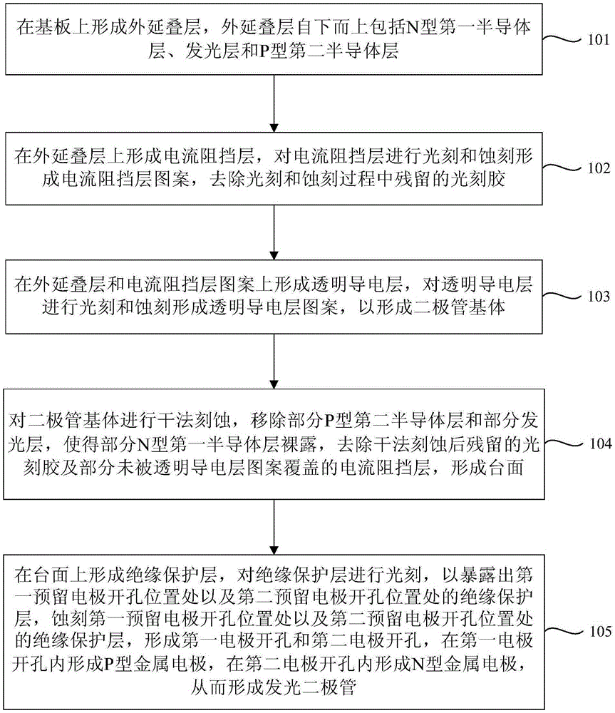
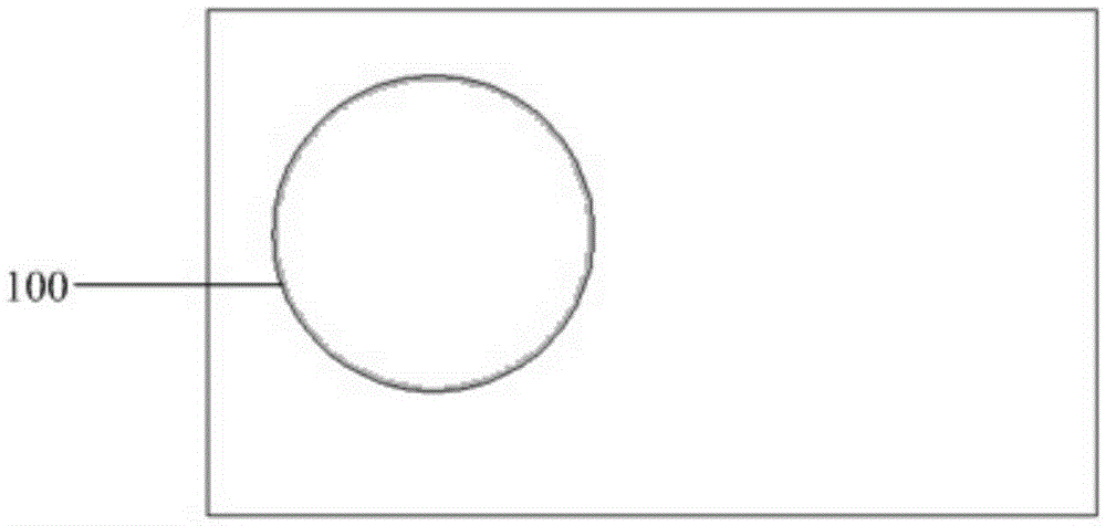
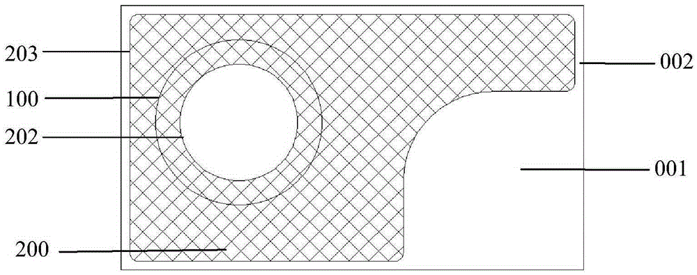
[0022] figure 1 It is a flow chart of an embodiment of the fabrication method of the GaN-based light-emitting diode of the present invention. figure 2 It is the pattern of the current blocking layer of an embodiment of the fabrication method of the GaN-based light emitting diode of the present invention. image 3 It is a schematic diagram of th...


PUM


Abstract

Embodiments of the invention provide a manufacturing method of a GaN-based light emitting diode. The method comprises the following steps of forming an epitaxial lamination on a substrate; forming a current barrier layer pattern and a transparent conducting layer pattern on the epitaxial lamination; carrying out dry etching so that a part of N-type first semiconductor layer is exposed so as to form a table board; forming an insulation protection layer on the table board, carrying out electrode lithography on the insulation protection layer so as to form a first electrode opening and a second electrode opening, and forming a metal electrode in each electrode opening so as to form a light emitting diode. By using the manufacturing method of the GaN-based light emitting diode, through adjusting lithography of each structure and an etching sequence, in a total process flow, the lithography only needs to be performed for three times so that the light emitting diode which has a same structure with the structure of the light emitting diode obtained through using a routine technology is acquired; manufacturing time of the light emitting diode is shortened; and material cost and production cost are reduced.

Description

technical field [0001] The invention relates to the fabrication technology of light-emitting diodes, in particular to a fabrication method of GaN-based light-emitting diodes. Background technique [0002] A light-emitting diode (Light-Emitting Diode, referred to as LED) is a semiconductor diode that emits light when the PN junction is under forward bias. LED has many advantages such as small size, light weight, firm structure, strong shock and earthquake resistance, long life, environmental protection and no pollution, and has developed into one of the most valued light source technologies in recent years. [0003] The manufacturing process of LED chips includes two parts: epitaxial growth and chip production: epitaxial growth refers to the growth of III-V semiconductor materials on substrate materials. Chip fabrication refers to the processing of chips after epitaxial growth to make them into LED light-emitting chips. Existing processing technologies usually include: firs...

Claims


Application Information

Patent Timeline
Patent Type & Authority Applications(China)
IPC IPC(8): H01L33/00H01L33/14H01L33/42H01L33/44
CPCH01L33/0075H01L33/145H01L33/42H01L33/44H01L2933/0016H01L2933/0025
Inventor 姚禹郑远志陈向东康建梁旭东
Owner EPITOP PHOTOELECTRIC TECH
Why Eureka
Try Eureka