Pixel structure and display panel

A pixel structure and display panel technology, applied in nonlinear optics, instruments, optics, etc., can solve the problems of difficult laser, difficult design of display panel, difficult repair of pixel structure, etc., and achieve the effect of high aperture ratio

Active Publication Date: 2016-02-03
AU OPTRONICS CORP
View PDF7 Cites 10 Cited by
  • Summary
  • Abstract
  • Description
  • Claims
  • Application Information

AI Technical Summary

Problems solved by technology

However, a certain standard distance needs to be kept between the above-mentioned multiple openings, so that the layout of the pixel structure is limited.
Therefore, under the premise of achieving high resolution, it is very difficult to design a display panel with a high aperture ratio by adopting the above-mentioned design of multiple color filter pattern openings.
In addition, under the consideration of increasing the aperture ratio, the area of ​​the opening of the color filter pattern in the overlapping area of ​​the pixel electrode and the sharing line is often designed to be small, but this makes it difficult to repair the pixel structure (that is, the laser is not easy to pass through the larger small color filter pattern opening), and the repair success rate is low

Method used


Image

  • Pixel structure and display panel
  • Pixel structure and display panel
  • Pixel structure and display panel

Examples


Embodiment Construction

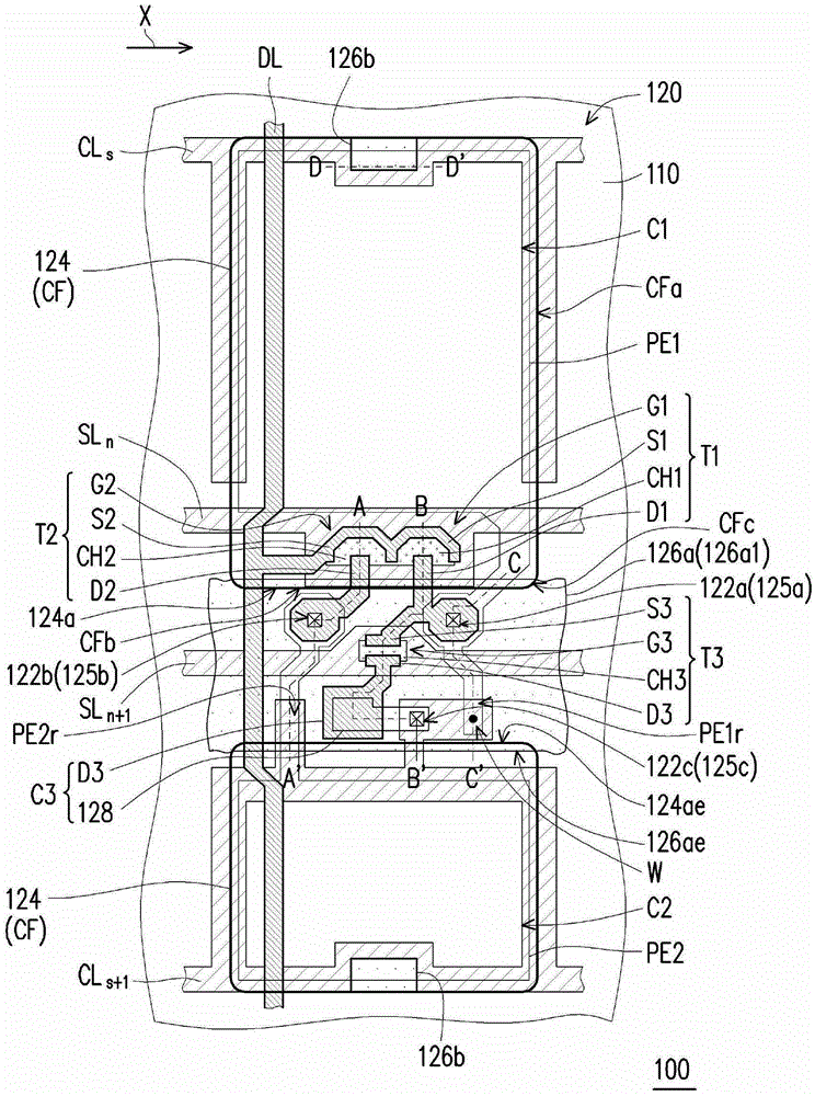
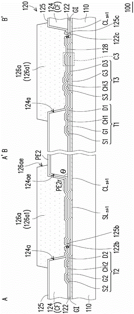
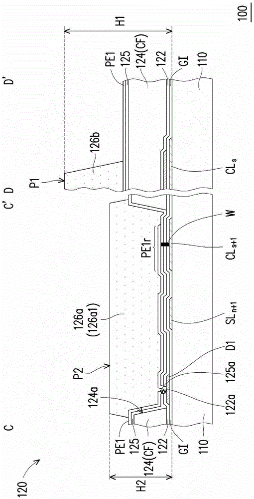
[0085] figure 1 It is a schematic top view of a pixel array substrate according to an embodiment of the present invention. Please refer to figure 1 The pixel array substrate 100 includes a first substrate 110 and a pixel structure 120 disposed on the first substrate 110 . In this embodiment, the first substrate 110 is, for example, a transparent substrate, and the material of the transparent substrate may be glass, quartz, organic polymer or other applicable materials. However, the present invention is not limited thereto. In other embodiments, the first substrate 110 may also be an opaque / reflective substrate, and the material of the opaque / reflective substrate may be conductive material, wafer, ceramic or other applicable materials. Material. It should be noted that although figure 1 Only one pixel structure 120 is shown as a representative, but those skilled in the art figure 1 The pixel structure 120 and the following description can be based on actual needs, and a pl...


PUM


Abstract

A pixel structure comprises a data line, a first scanning line, a sharing line, a first active element, a second active element, an insulation layer coating the first active element and the second active element, a colorful filtering pattern arranged on the insulation layer, a first pixel electrode and a second pixel electrode arranged on the colorful filtering pattern and a protection pattern. The colorful filtering pattern has a groove. The first pixel electrode fills in the groove so as to electrically connect with the first active element. The first pixel electrode has one portion located in the groove and configured to overlap with the sharing line. The second pixel electrode fills in the groove so as to electrically connect with the second active element. The second pixel electrode has one portion located in the groove and configured to overlap with the sharing line. The protection pattern fills in the groove so as to cover partial first pixel electrode and second pixel electrode. The protection pattern is insulation transparent material.

Description

technical field [0001] The present invention relates to a semiconductor structure and a semiconductor device, and in particular to a pixel structure and a display panel. Background technique [0002] With the advancement of technology, the bulky cathode ray tube (CathodeRayTube, CRT) display has gradually entered the history. Compact flat-panel displays, such as: Liquid Crystal Display (LCD), Organic Light Emitting Diode display (OLED display), Electro-Phoretic Display (EPD), Plasma Display Panel (PDP), etc. It replaced the cathode ray tube display and became the mainstream of the display. [0003] In recent years, the industry has proposed a technology of integrating color filter patterns on a pixel array substrate (Color Filter on Array, COA). A display panel can be formed by assembling the COA substrate and another opposite substrate, and filling the display medium between them. Since the color filter pattern is directly formed on the pixel array substrate, the alignme...

Claims


Application Information

Patent Timeline
Patent Type & Authority Applications(China)
IPC IPC(8): G02F1/1362G02F1/1343G02F1/1335
CPCG02F1/133514G02F1/134309G02F1/136227G02F1/136286
Inventor 林庭谊江俊毅廖达文
Owner AU OPTRONICS CORP
Why Eureka
Try Eureka