Quantum dot light-emitting field effect transistor and preparation method thereof

A field-effect transistor and quantum dot light-emitting technology, which is applied in the manufacture of semiconductor/solid-state devices, electric solid-state devices, semiconductor devices, etc., can solve the problems of large hole injection barrier, complicated preparation process and high production cost of QLED devices, and achieve The effect of overcoming the energy barrier, simplifying the preparation process and prolonging the service life

Inactive Publication Date: 2016-02-03
TCL CORPORATION
View PDF3 Cites 5 Cited by
  • Summary
  • Abstract
  • Description
  • Claims
  • Application Information

AI Technical Summary

Problems solved by technology

[0004] The purpose of the present invention is to provide a quantum dot light-emitting field-effect transistor, which aims to solve the problems of complex preparation process and high manufacturing cost caused by making QLED and FET on the same substrate and directly using FET to drive QLED in the prior art, and by The obtained QLED device has the problem of low luminous efficiency due to the large hole injection barrier

Method used


Image

  • Quantum dot light-emitting field effect transistor and preparation method thereof
  • Quantum dot light-emitting field effect transistor and preparation method thereof
  • Quantum dot light-emitting field effect transistor and preparation method thereof

Examples


Embodiment Construction

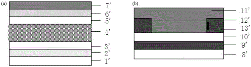
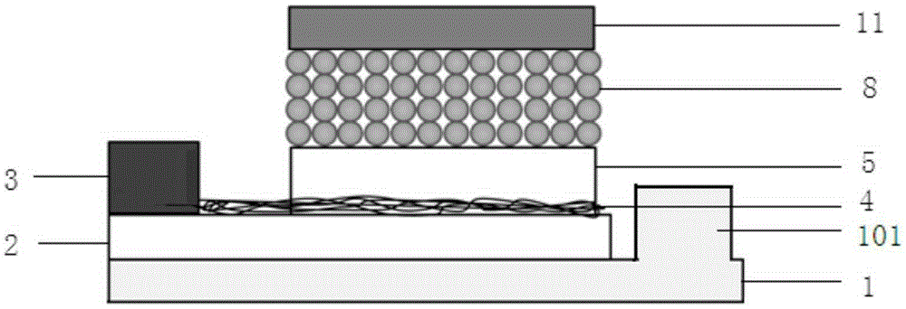
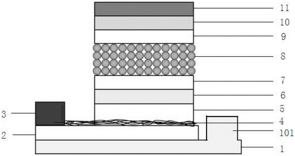
[0026] In order to make the technical problems, technical solutions and beneficial effects to be solved by the present invention clearer, the present invention will be further described in detail below in conjunction with the accompanying drawings and embodiments. It should be understood that the specific embodiments described here are only used to explain the present invention, not to limit the present invention.

[0027] combine Figure 2-4 , the embodiment of the present invention provides a quantum dot light-emitting field effect transistor, including a gate 1, and the gate 1 protrudes on one side to form a gate boss 101;

[0028] an insulating layer 2 disposed on the gate 1, and the insulating layer 2 is not in contact with the gate protrusion 101;

[0029] a source 3 disposed on the side of the insulating layer 2 opposite to the gate protrusion 101;

[0030] A carbon nanotube layer 4 disposed on the insulating layer 2 and connected to the source 3;

[0031] a semicond...


PUM

PropertyMeasurementUnit
Thicknessaaaaaaaaaa

Abstract

The invention is suitable for the field of semiconductor technology, and provides a quantum dot light-emitting field effect transistor and a preparation method thereof. The quantum dot light-emitting field effect transistor comprises the components of a gate electrode which projects from one side and forms a gate electrode boss; an insulating layer which is arranged on the gate electrode and does not contact with the gate electrode boss; a source electrode which is arranged on the insulating layer at the side that faces the gate electrode boss; a carbon nanotube layer which is arranged on the insulating layer and is connected with the source electrode; a semiconductor layer which is arranged on the carbon nanotube layer and does not contact with the source electrode; and a quantum dot light-emitting layer and a drain electrode which are successively laminated on the semiconductor layer.

Description

technical field [0001] The invention belongs to the technical field of semiconductors, and in particular relates to a quantum dot light-emitting field-effect transistor and a preparation method thereof. Background technique [0002] Quantum dot light-emitting diode (QLED) is a high-performance light-emitting device that uses nanoscale quantum dots as light-emitting materials, and it has great potential application value in the display field. QLED includes a quantum dot light-emitting layer and electrodes. In order to achieve high-performance quantum dot electroluminescence, other auxiliary functional layers are usually provided to help carriers be injected into quantum dots efficiently. They are respectively carrier injection layers (electron injection layers) , hole injection) and transport layers (electron transport, hole transport), figure 1 (a) shows a typical QLED device structure, where 1'-7' are anode, hole injection layer, hole transport layer, quantum dot light-emi...

Claims


Application Information

Patent Timeline
IPC IPC(8): H01L51/52H01L51/56
CPCH10K50/30H10K71/00
Inventor 肖标付东闫晓林
Owner TCL CORPORATION
Why Eureka
Try Eureka