Negative electrode active material for electric device and electric device using same
A technology for negative active materials and electrical equipment, applied in the direction of active material electrodes, non-aqueous electrolyte storage batteries, negative electrodes, etc., can solve the problems of large expansion and contraction at the negative electrode, reduced electrode cycle life, and inability to obtain charge and discharge capacity, etc.
- Summary
- Abstract
- Description
- Claims
- Application Information
AI Technical Summary
Problems solved by technology
Method used
Image

Examples
Embodiment
[0206] The present invention is illustrated in further detail using the following examples. However, the protection scope of the present invention is not limited to the following examples.
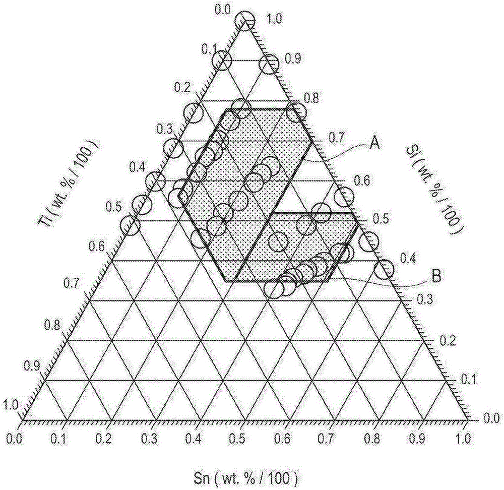
[0207] First, as a reference example, performance evaluation was performed on the Si alloy represented by the above chemical formula (1) constituting the negative electrode active material for electrical equipment of the present invention.
reference example A
[0208] (Reference Example A): For Si x sn y Ti z A a performance evaluation of
[0209] [1] Production of negative electrode
[0210] As the sputtering device, a 3-element DC magnetron sputtering device (manufactured by Daiwa Ki Kogyo Co., Ltd., combined sputtering coating device, gun-sample distance: about 100mm) using an independent control method was used. On the substrate (current collector) that the nickel foil of thickness 20 μm forms will have the thin film of the negative electrode active material alloy of each composition film-forming respectively, thus obtain a total of 40 kinds of negative electrode samples (reference example 1-1~1-26 and reference example 1-1~1-26 and reference Example 1'-1 to 1'-14).
[0211] (1) Target (manufactured by High Purity Chemical Laboratory Co., Ltd., purity: 4N)
[0212] Si: 50.8mm diameter, 3mm thickness (with a 2mm thick oxygen-free copper backing plate)
[0213] Sn: 50.8mm diameter, 5mm thickness
[0214] Ti: 50.8mm diameter...
reference example B
[0248] (Reference Example B): For Si x sn y Zn z A a performance evaluation of
[0249] [1] Production of negative electrode
[0250] "Ti: 50.8 mm diameter, 5 mm thickness" of the target in (1) of reference example A was changed to "Zn: 50.8 mm diameter, 3 mm thickness." Furthermore, "Ti (0-150W)" of the DC power supply in (2) was changed to "Zn (0-150W)". A total of 46 kinds of negative electrode samples (Reference Examples 2-1 to 2-32 and Reference Examples 2'-1 to 2'-14) were prepared by the same method as Reference Example A except for the above changes.
[0251] That is, using the above-mentioned Si target, Sn target, and Zn target, the sputtering time was fixed at 10 minutes, and the power of the DC power supply was varied within the above-mentioned range. In this way, an alloy thin film in an amorphous state was formed on a Ni substrate, and negative electrode samples including alloy thin films of various compositions were obtained.
[0252] It should be noted th...
PUM
| Property | Measurement | Unit |
|---|---|---|
| thickness | aaaaa | aaaaa |
| diameter | aaaaa | aaaaa |
| diameter | aaaaa | aaaaa |
Abstract
Description
Claims
Application Information
 - R&D Engineer
- R&D Manager
- IP Professional
- Industry Leading Data Capabilities
- Powerful AI technology
- Patent DNA Extraction
Browse by: Latest US Patents, China's latest patents, Technical Efficacy Thesaurus, Application Domain, Technology Topic.
© 2024 PatSnap. All rights reserved.Legal|Privacy policy|Modern Slavery Act Transparency Statement|Sitemap