Eureka AIR delivers breakthrough ideas for toughest innovation challenges, trusted by R&D personnel around the world.

Wafer corrosion device

A technology for etching devices and wafers, which is applied in the fields of electrical components, semiconductor/solid-state device manufacturing, circuits, etc., can solve problems such as uneven temperature, large consumption of chemical liquid, and differences in uniformity of wafer surface corrosion, so as to improve the utilization rate , Mention the uniformity and ensure the effect of uniformity

Inactive Publication Date: 2016-02-17
SHANGHAI VASTITY ELECTRONICS TECH
View PDF9 Cites 10 Cited by
  • Summary
  • Abstract
  • Description
  • Claims
  • Application Information

AI Technical Summary

Problems solved by technology

[0003] At present, there are two main types of wafer etching devices in the market, one is a single wafer etching device, and the other is a multi-wafer etching device. The single wafer etching device only rotates a single wafer by spraying chemical liquid Wafers are etched, the advantage is that the corrosion uniformity of the wafers is better, but the main disadvantages are low efficiency, large consumption of chemical liquid, and do not use industrial scale production
Therefore, in the industrial production process, multi-chip etching devices are mostly used. In the multi-chip etching device, multiple wafers are put into the wafer cassette and put into the etching tank. During the multi-chip etching process, due to the different concentration of the chemical solution in the tank Uniformity, the temperature of the upper and lower sides of the tank is uneven, and the bubbles generated during the wafer corrosion process adhere, resulting in a large difference in the corrosion uniformity of the wafer surface

Method used


Image

  • Wafer corrosion device
  • Wafer corrosion device
  • Wafer corrosion device

Examples


Embodiment 1

[0045] Embodiment 1, the corrosion of wafer surface removal oxide layer

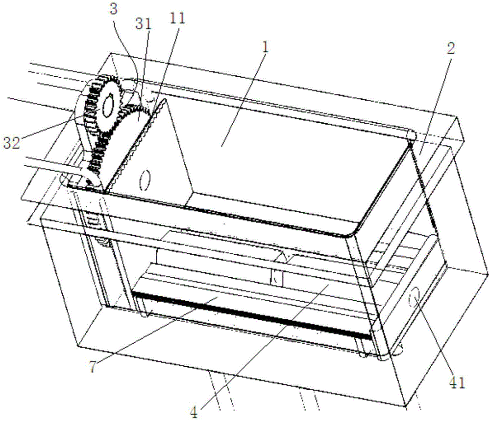
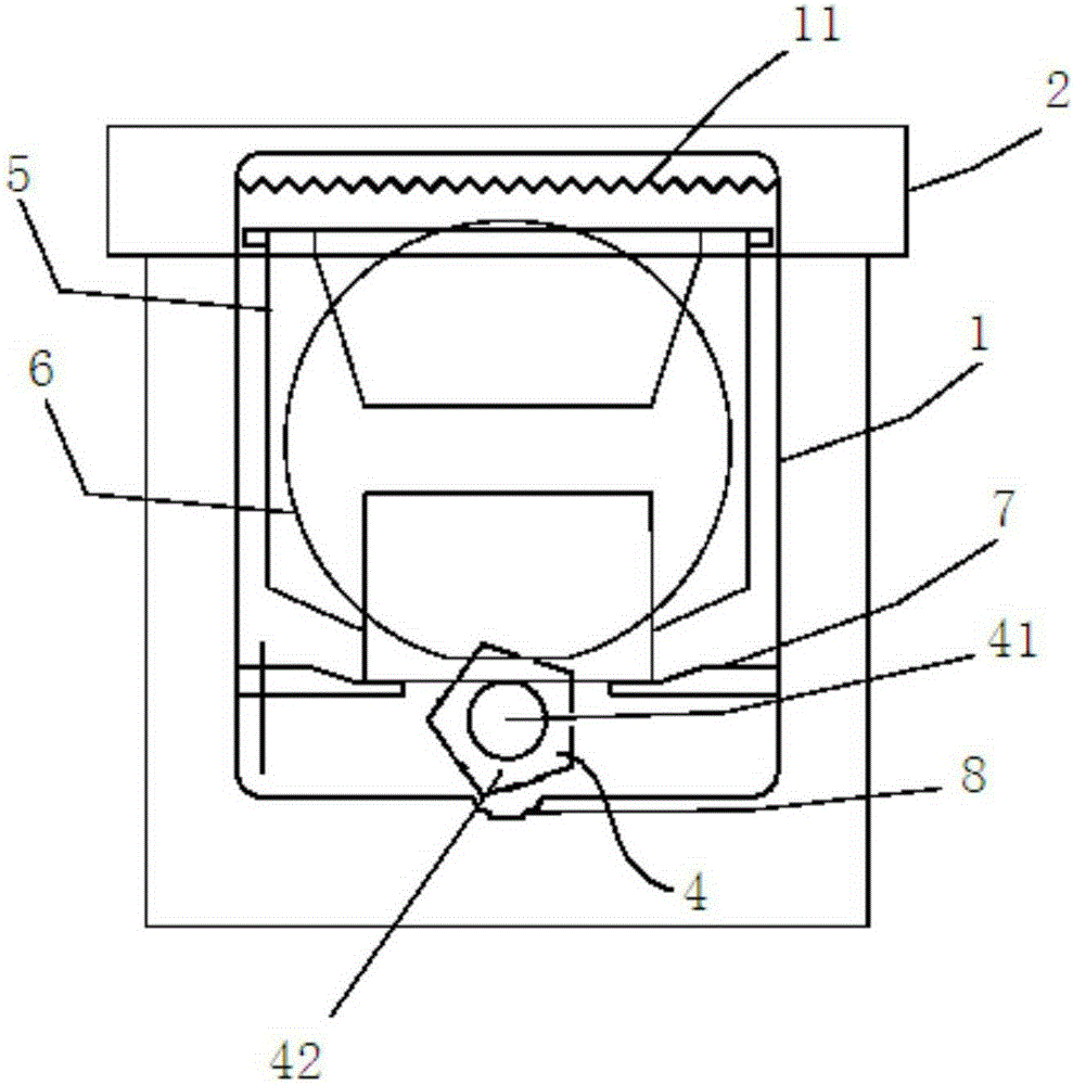
[0046] In this embodiment, the corrosion solution used is %49HF (hydrofluoric acid), and the inner box body 1 and the outer box body 2 are formed by thermal welding of PVDF material. The drive unit adopts a frequency conversion motor, the polygonal rotating column adopts a regular pentagonal rotating column, the metal shaft of the regular pentagonal rotating column is made of metal titanium, and the regular pentagonal hollow column is made of PTFE material.

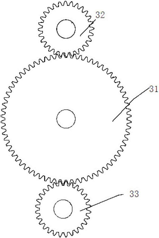
[0047] Put the wafer cassette 5 into the inner box 1, inject %49HF (hydrofluoric acid) into the inner box 1, drive the frequency conversion motor to rotate, the polygonal rotating column follows the transmission gear and rotate forward, the prism between the wafer and the regular pentagonal rotating column contact, the wafer 6 is rotated, and the overflow pump is started at the same time, so that the %49HF (hydrofluoric acid) throws the wafer up and...

Embodiment 2

[0048] Embodiment 2: Corrosion of wafer 6 surface stripping surface photoresist

[0049] In this embodiment, the etching solution used is EKC (synthetic organic chemical solution). The inner box 1 and the outer box 2 are welded by 316 stainless steel, the transmission mechanism is made of 316 stainless steel, the transmission mechanism is connected to the frequency conversion motor, the polygonal rotating column adopts the regular pentagonal rotating column, and the regular pentagonal rotating column The metal shaft is made of titanium, and the regular pentagonal hollow column is made of 316 stainless steel. The stainless steel material can resist the corrosion of EKC chemical liquid. At the same time, the outer box 2 is equipped with a film heater to heat the EKC chemical liquid to make the EKC chemical liquid reach 90°C, because the degumming effect is best when the EKC chemical liquid is at 90°C.

[0050] After the wafer cassette 5 is put into the inner box 1, EKC chemical...


PUM


Abstract

The invention relates to the technical field of semiconductor manufacturing, in particular to a wafer corrosion device. The wafer corrosion device is applied to wafer surface substance corrosion processing. The wafer corrosion device comprises an inner box, an outer box, a transmission device and an overflowing pump, wherein a detachable cavity with a wafer box containing a plurality of wafers is formed inside the inner box, and a groove matched with a polygonal rotating column is formed in the bottom of the inner box; the outer box and the inner box are arranged at a preset interval, and the outer box completely covers the inner box; the driving end of the transmission device is connected with a driving unit, and the output end of the transmission device is connected with the polygonal rotating column; the overflowing pump is arranged inside the inner box and used for providing pushing force for pushing a corrosion solution contained inside the inner box to overflow into the outer box. When the overflowing pump pushes the corrosion solution to overflow into the outer box, the polygonal rotating column is driven by the transmission device to drive the wafers to rotate in the flowing corrosion solution.

Description

technical field [0001] The invention relates to the technical field of semiconductor manufacturing, in particular to a wafer etching device. Background technique [0002] In the wafer manufacturing process of the semiconductor industry, it is necessary to etch the wafer before ion implantation, diffusion, and photolithography. The common etching is to remove the surface photoresist and remove the surface silicon dioxide oxide layer. After the wafer enters the etching tank , the chemical liquid etches the surface of the wafer to remove excess substances on the surface. [0003] At present, there are two main types of wafer etching devices in the market, one is a single wafer etching device, and the other is a multi-wafer etching device. The single wafer etching device only rotates a single wafer by spraying chemical liquid The wafer is etched, which has the advantage of better corrosion uniformity of the wafer, but the main disadvantages are low efficiency, high consumption ...

Claims


Application Information

Patent Timeline
Patent Type & Authority Applications(China)
IPC IPC(8): H01L21/67
CPCH01L21/67075H01L21/67086
Inventor 张欢
Owner SHANGHAI VASTITY ELECTRONICS TECH
Why Eureka
Eureka Blog
Learn More