Production method of local-thick copper PCB

A production method and local thick copper technology are applied in the fields of printed circuit manufacturing, reinforcement of conductive patterns, and secondary treatment of printed circuits. Yield rate, simplification of process flow and improvement of product quality

Inactive Publication Date: 2016-02-17
东莞森玛仕格里菲电路有限公司
View PDF3 Cites 19 Cited by
  • Summary
  • Abstract
  • Description
  • Claims
  • Application Information

AI Technical Summary

Problems solved by technology

The main production defects of this type of PCB are: 1. The method of making PCB with high and low copper thickness is long. In order to achieve a local copper thickness that is thicker than other places, it is necessary to repeat the processes of electroplating, film sticking, film removal, and etching many times, and the process is complicated. , prone to defects and scrapping, low yield rate
2. The height difference area is easy to cause the secondary film to be weak

Method used


Image

  • Production method of local-thick copper PCB
  • Production method of local-thick copper PCB
  • Production method of local-thick copper PCB

Examples


Embodiment Construction

[0025] The present invention will be further described below in conjunction with accompanying drawing and preferred embodiment, see Figure 1-8 As shown, the manufacturing method of local thick copper PCB includes the following steps:

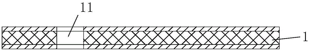
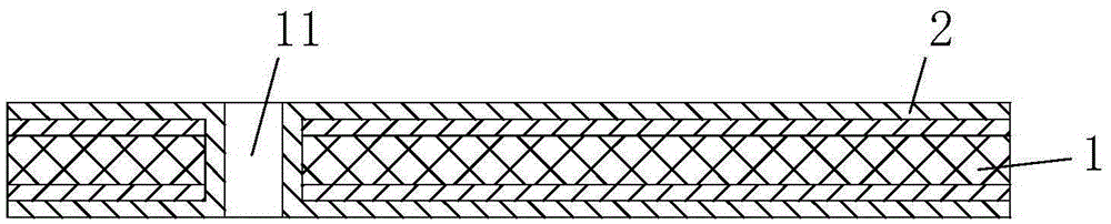
[0026] 1. Drilling steps: Drill hole position 11 on circuit board 1; circuit board 1 is a double-sided or multi-layer circuit board; hole position 11 is a conduction hole or positioning hole;

[0027] 2. Primary copper plating step: carry out copper sinking and electroplating on the circuit board 1, so that the upper and lower surfaces of the circuit board 1 and the walls of hole 11 are plated with a primary copper plating layer 2;

[0028] 3. Secondary copper plating step: Paste a dry film 3 on the area of ​​the circuit board 1 that does not require secondary copper plating, expose and develop, and then perform a secondary copper plating treatment on the circuit board 1, so that the circuit board 1 needs secondary copper plating. The copper-p...


PUM


Abstract

The invention relates to technical field of PCBs and particularly relates to a production method of a local-thick copper PCB. The production method comprises the following steps of A, drilling, namely drilling on a circuit board; B, primary copper plating; C, secondary copper plating, namely pasting a primary dry film, exposing, developing, and then, carrying out secondary copper plating treatment on the circuit board; D, local thick copper plating, namely pasting a secondary dry film, exposing, developing, and then, carrying out thick copper plating treatment on the circuit board; E, secondary dry film deplating; F, tin plating; and G, primary dry film deplating, etching and tin deplating treatment. According to the production method, secondary copper plating is carried out through covering a region to be etched by using the primary dry film, and then, the region except for the regions where thick copper is needed to be plated are covered by the secondary dry film, so that the process is continuous, local thick copper plating can be realized favorably through only selecting the dry films with proper thicknesses and controlling proper film deplating parameters, and the process flow is simplified; the films can be pasted on a plane every time, so that the films are firmly pasted, the rate of good products is increased, and the quality of the local-thick copper PCB is improved.

Description

Technical field: [0001] The invention relates to the technical field of PCB boards, in particular to a method for manufacturing a local thick copper PCB. Background technique: [0002] The design and application of existing circuit boards are becoming more and more specialized. Some circuit boards have inconsistent copper requirements for circuit positions and copper plating. The copper plating layer of some parts is required to be thicker than other parts. It can control the copper thickness of the whole surface to be consistent, and it is difficult to meet the special surface copper requirements of local positions. At present, there are almost no mature and simple processes for making local thick copper PCBs, especially PCBs with a height difference of more than 2 oz (ounces). The main production defects of this type of PCB are: 1. The method of making PCB with high and low copper thickness is long. In order to achieve a local copper thickness that is thicker than other p...

Claims


Application Information

Patent Timeline
Patent Type & Authority Applications(China)
IPC IPC(8): H05K3/24
CPCH05K3/243H05K2201/098
Inventor 刘慧民周勇胜
Owner 东莞森玛仕格里菲电路有限公司
Why Eureka
Try Eureka