Preparation method of NiAu projection and NiAu projection assembly

A manufacturing method and a technology of bumps, which are applied in the direction of electrical components, electric solid devices, semiconductor devices, etc., can solve the problems of accelerating seed layer etching, reducing the bonding area of ​​bumps and metal layers, and reducing the bonding force, so as to avoid bonding Reduction of area and binding force, effect of avoiding galvanic reaction

Active Publication Date: 2016-02-24
CHIPMORE TECH CORP LTD
View PDF5 Cites 11 Cited by
  • Summary
  • Abstract
  • Description
  • Claims
  • Application Information

AI Technical Summary

Problems solved by technology

However, some chips with special functions require special bump structures, such as nickel-gold bumps, but if they are to be combined with the commonly used titanium-tungsten + gold, titanium, or titanium-tungsten + copper seed layers, after the bumps are generated When the excess seed layer on the outside of the bottom of the bump is removed by wet etching, due to the difference in metal potential between copper, nickel and gold, coupled with the assistance of the wet chemical solution, the copper metal layer undergoes a galvanic reaction, which accelerates the etching of the seed layer. In addition, it will also lead to excessive undercutting of the entire nickel bump, reducing the bonding area between the bump and the metal layer, resulting in a decrease in the bonding force, and then causing the bump to peel off the wafer prematurely

Method used


Image

  • Preparation method of NiAu projection and NiAu projection assembly
  • Preparation method of NiAu projection and NiAu projection assembly
  • Preparation method of NiAu projection and NiAu projection assembly

Examples


Embodiment Construction

[0029] Hereinafter, the present invention will be described in detail with reference to the embodiments shown in the drawings. The following is a preferred embodiment of the present invention.

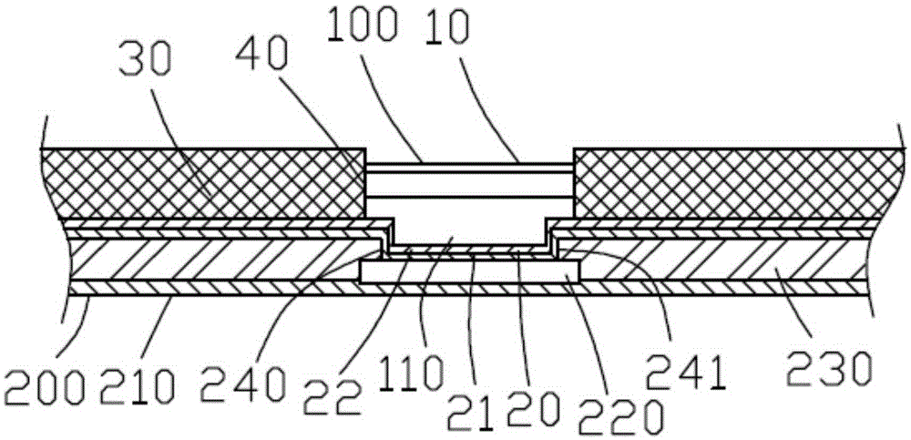
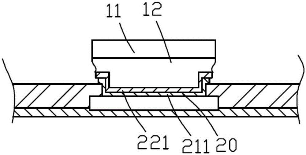
[0030] See figure 1 , image 3 , The present invention relates to a bump assembly 100 made of nickel and gold, which is protrudingly formed on the semiconductor wafer assembly 200. The bump assembly 100 includes a nickel-gold bump 10 with a protruding portion 110 at the lower end, which is bonded between the bump 10 and the wafer assembly 200, that is, the upper and lower surfaces of the bump 10 are respectively connected to the bump 10. The bottom end of the metal layer 20 is attached to the top end of the wafer assembly 200.

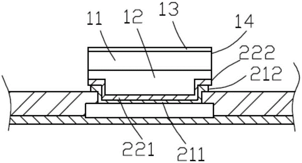
[0031] The bump 10 includes a gold metal layer 11, a nickel metal layer 12 disposed under the gold metal layer 11, and a reserve layer 13 disposed on the gold metal layer 11. The metal layer 20 includes a seed metal layer 221 sputtered on the bottom end of the bum...


PUM


Abstract

The invention provides a preparation method of a NiAu projection. The method comprises that a Ti or TiW metal layer and an Au metal layer are formed between a wafer and the NiAu projection from top to bottom, the Au metal layer outside the projection is removed from top to bottom in a physical dry etching manner, the Ti or TiW metal layer is removed via a wet etching manner, and reaction of a galvanic cell and excessive etching of the Ni material of the projection caused by the wet etching manner are avoided. The invention also provides a NiAu projection assembly which comprises the projection, a seed metal layer and a substrate metal layer, wherein the projection comprises a reserved layer, the Au metal layer and a Ni metal layer are successively from top to bottom, the seed metal layer and the substrate metal layer are arranged at the bottom of the projection, the lateral side of the Au metal layer and the lateral side of the projection are leveled in the vertical direction, and relatively large combination area and combination force between the projection and the wafer are ensured.

Description

Technical field [0001] The invention relates to the field of integrated circuits, in particular to a method for manufacturing nickel-gold bumps and a nickel-gold bump assembly. Background technique [0002] Bumps are often used in integrated circuit wafer packaging technology. As more and more wafers need to change the original design and production to adapt to different packaging modes, it is necessary to make corresponding bump patterns on the wafers to meet At the same time, the demand for bump structures and materials is also increasing. [0003] In the process of making bumps, a metal substrate layer and a seed layer need to be formed on the wafer, and then bumps are formed on the seed layer. After the bumps are made, two extra metal layers outside the bumps need to be removed. At present, bumps are mostly made of gold, copper, copper-nickel gold, etc. Generally, gold bumps are matched with a seed layer made of titanium tungsten + gold, and bumps of other materials are matche...

Claims


Application Information

Patent Timeline
Patent Type & Authority Applications(China)
IPC IPC(8): H01L21/60H01L21/3213H01L23/48
CPCH01L2224/11H01L24/10H01L21/3213H01L21/32131H01L23/48H01L24/11H01L24/12H01L2224/10H01L2224/12105
Inventor 梅嬿
Owner CHIPMORE TECH CORP LTD
Why Eureka
Try Eureka